
The semiconductor industry is continuously pushing the boundaries of performance, power efficiency, and integration. As traditional transistor scaling becomes increasingly challenging, advanced packaging technologies have emerged as a critical enabler of next-generation computing systems.
Among these technologies, 2.5D IC Packaging and 3D IC Packaging have gained significant attention. Both approaches enable multiple semiconductor dies to work together within a single package, delivering higher bandwidth, improved performance, and reduced power consumption. However, their architectures, manufacturing methods, and application areas differ considerably.
Understanding the Need for Advanced Packaging
For many years, semiconductor performance improvements relied primarily on Moore’s Law. However, shrinking transistor dimensions has become increasingly expensive and technically complex.
Modern applications such as:
- Artificial Intelligence (AI)
- High-Performance Computing (HPC)
- Data Centers
- Autonomous Vehicles
- 5G Infrastructure
- Edge Computing
require significantly higher processing power and memory bandwidth than conventional packaging solutions can provide.
Advanced packaging addresses these challenges by integrating multiple dies into a single package, enabling faster communication and improved system-level performance.
What is 2.5D IC Packaging?
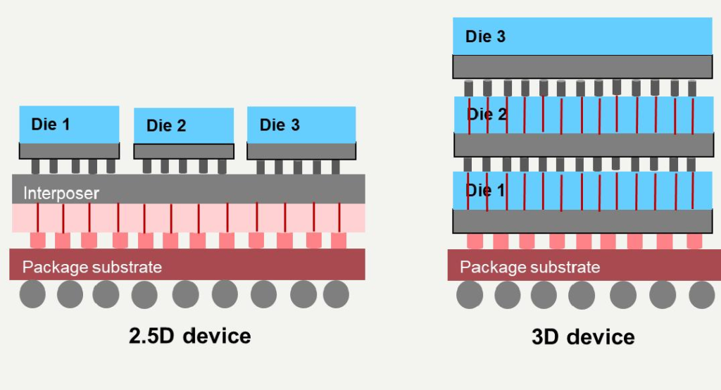
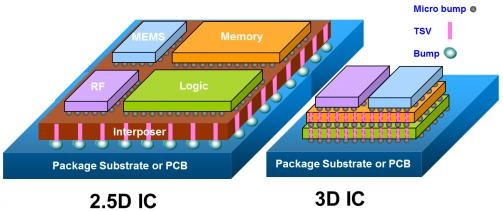
2.5D IC packaging places multiple semiconductor dies side-by-side on a silicon interposer. The interposer acts as a high-density communication layer that connects the dies through thousands of fine interconnects.
Unlike traditional packaging, where chips communicate through longer PCB traces, the interposer significantly shortens signal paths, resulting in higher bandwidth and lower latency.
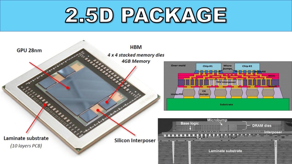
Key Features of 2.5D Packaging
- Dies are placed horizontally on an interposer.
- Uses Through-Silicon Vias (TSVs) within the interposer.
- Supports high-speed die-to-die communication.
- Commonly used with High Bandwidth Memory (HBM).
Advantages
- High memory bandwidth
- Improved signal integrity
- Lower communication latency
- Better thermal management
- Easier manufacturing compared to 3D stacking
Challenges
- Expensive silicon interposers
- Larger package footprint
- Increased assembly complexity
What is 3D IC Packaging?
3D IC packaging stacks multiple semiconductor dies vertically and connects them using Through-Silicon Vias (TSVs), micro-bumps, or hybrid bonding technologies.
By stacking dies directly on top of one another, communication distances become extremely short, leading to substantial improvements in performance and power efficiency.
Key Features of 3D Packaging
- Vertical die stacking
- TSV-based interconnects
- Hybrid bonding support
- Extremely high integration density
Advantages
- Maximum integration density
- Reduced interconnect length
- Lower power consumption
- Higher bandwidth
- Smaller package size
Challenges
- Thermal management difficulties
- Higher manufacturing complexity
- Yield challenges
- Increased production costs
Key Differences Between 2.5D and 3D IC Packaging
1. Die Arrangement
2.5D IC Packaging
- Dies are positioned side-by-side on a silicon interposer.
3D IC Packaging
- Dies are stacked vertically to maximize integration density.
2. Interconnect Technology
2.5D IC Packaging
- Communication occurs through a silicon interposer.
3D IC Packaging
- Communication occurs through TSVs and direct die-to-die bonding.
3. Integration Density
2.5D IC Packaging
- High integration density.
3D IC Packaging
- Extremely high integration density due to vertical stacking.
4. Performance
2.5D IC Packaging
- Delivers excellent bandwidth and low latency.
3D IC Packaging
- Provides even higher bandwidth and lower latency because of shorter signal paths.
5. Power Efficiency
2.5D IC Packaging
- More power-efficient than traditional packaging.
3D IC Packaging
- Superior power efficiency due to direct vertical connections.
6. Thermal Management
2.5D IC Packaging
- Easier heat dissipation.
3D IC Packaging
- More challenging because heat can become trapped between stacked dies.
7. Package Size
2.5D IC Packaging
- Requires a larger footprint.
3D IC Packaging
- Enables compact package designs.
8. Manufacturing Complexity
2.5D IC Packaging
- Moderate manufacturing complexity.
3D IC Packaging
- Significantly more complex fabrication and assembly process.
9. Cost
2.5D IC Packaging
- Lower overall cost.
3D IC Packaging
- Higher cost due to advanced manufacturing requirements.
How Communication Improves in Advanced Packaging
One of the primary advantages of both technologies is the reduction in communication distance between semiconductor dies.
Traditional Packaging
Signals travel through long PCB traces, resulting in:
- Higher latency
- Greater power consumption
- Reduced bandwidth
2.5D Packaging
Signals travel through the silicon interposer, enabling:
- Faster communication
- Improved bandwidth
- Better signal integrity
3D Packaging
Signals move vertically through TSVs, providing:
- Ultra-short communication paths
- Extremely low latency
- Maximum bandwidth efficiency
This makes advanced packaging highly attractive for AI accelerators and high-performance computing systems.
Applications of 2.5D IC Packaging
High-Performance Computing (HPC)
Large processors require massive memory bandwidth. 2.5D packaging enables efficient integration of compute dies and HBM memory.
AI Accelerators
Modern AI workloads demand rapid data movement between processors and memory.
Data Centers
Advanced processors benefit from higher bandwidth and lower power consumption.
Networking Equipment
High-speed networking ASICs use 2.5D packaging to handle large data transfers efficiently.
FPGAs
Many high-end FPGA solutions use interposer-based architectures for enhanced connectivity.
Applications of 3D IC Packaging
Mobile Processors
Smartphones and portable devices benefit from compact package sizes.
Artificial Intelligence
3D integration enables greater compute density and improved energy efficiency.
Memory Technologies
Many advanced memory products use vertical stacking.
Examples include:
- 3D NAND Flash
- Stacked DRAM
- High-density memory solutions
Edge Computing
Compact and efficient packages make 3D ICs ideal for edge devices.
Automotive Electronics
Autonomous driving platforms increasingly require dense, power-efficient computing systems.
Emerging Industry Trends
Chiplet-Based Design
Large monolithic chips are increasingly being replaced by smaller chiplets interconnected within advanced packages.
Hybrid Bonding
Hybrid bonding provides finer interconnect pitches and improved electrical performance compared to traditional micro-bumps.
Heterogeneous Integration
Future systems will combine:
- Logic
- Memory
- RF
- Analog
- Photonics
within a single package.
Advanced Memory Architectures
Future memory standards such as HBM4 and beyond will rely heavily on advanced packaging technologies.
AI-Driven Package Optimization
Machine learning is being used to optimize:
- Routing
- Thermal management
- Power delivery
- Package reliability
Conclusion
2.5D and 3D IC packaging represent two of the most important advancements in modern semiconductor engineering. While 2.5D packaging focuses on high-bandwidth communication through side-by-side die integration, 3D packaging achieves unparalleled density and efficiency through vertical stacking. As demand for AI, HPC, data centers, and intelligent edge devices continues to grow, both technologies will remain essential for overcoming the limitations of traditional semiconductor scaling and driving the future of advanced computing.