
The semiconductor industry is rapidly approaching the physical limits of traditional lithography techniques. As chip designs move toward 2 nm and beyond, manufacturers require more precise patterning solutions. This demand has led to the development of High-NA EUV Lithography, a next-generation technology designed to extend Moore’s Law and enable continued transistor scaling.
High-NA EUV is not just an improvement it is a fundamental shift in how advanced chips are manufactured.
What is High-NA EUV Lithography?
High-NA EUV (Extreme Ultraviolet Lithography) is an advanced semiconductor patterning technology that uses 13.5 nm wavelength light with a significantly higher numerical aperture (NA ≈ 0.55).
Extreme Ultraviolet Lithography
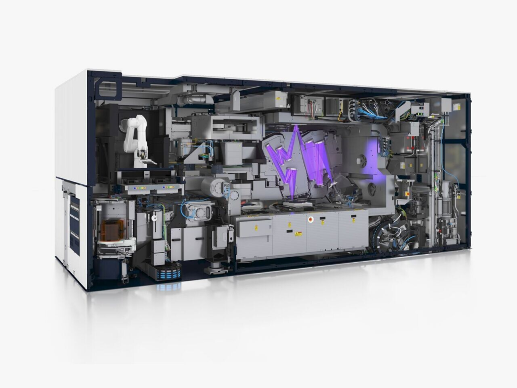
High-NA EUV Lithography
The term NA (Numerical Aperture) refers to the ability of the optical system to focus light. A higher NA allows:
- Smaller feature sizes
- Improved resolution
- Better pattern fidelity
In simple terms, High-NA EUV enables chipmakers to print much smaller and more complex transistor structures than current EUV systems.
Why High-NA EUV is Needed
As semiconductor nodes shrink, traditional EUV lithography (0.33 NA) faces limitations:
Key challenges in current EUV:
- Resolution constraints at sub-3nm nodes
- Increased reliance on multi-patterning
- Higher manufacturing complexity and cost
- Line-edge roughness affecting transistor performance
High-NA EUV addresses these issues by enabling single-exposure patterning for extremely small geometries.
This makes it essential for:
- Advanced AI processors
- High-performance computing (HPC) chips
- Next-generation mobile SoCs
How High-NA EUV Lithography Works
High-NA EUV systems are based on reflective optics, since EUV light cannot pass through lenses.
Key working principles:
- Extreme ultraviolet light source (13.5 nm)
- Multilayer reflective mirrors
- Anamorphic optical design (different scaling in X and Y axes)
- Ultra-high vacuum environment
Unlike conventional systems, High-NA EUV uses larger and more complex mirrors to achieve sharper imaging and improved resolution.
The result is extremely precise wafer patterning at atomic-scale dimensions.
Advantages of High-NA EUV Technology
High-NA EUV brings major improvements to semiconductor manufacturing:
1. Superior Resolution
Enables patterning below 2 nm technology nodes.
2. Reduced Process Complexity
Eliminates multiple patterning steps used in current EUV.
3. Improved Yield and Accuracy
More precise features reduce defects and variability.
4. Better Performance Efficiency
Allows higher transistor density and lower power consumption.
These advantages make High-NA EUV a key enabler for future chip generations.
Challenges and Industry Barriers
Despite its potential, High-NA EUV faces several challenges:
High Cost of Manufacturing Equipment
Each system costs hundreds of millions of dollars, limiting early adoption.
Complex Engineering Requirements
- Advanced vibration control
- Ultra-clean fabrication environments
- Extremely precise optical alignment
Resist and Material Limitations
Photoresist materials must handle extremely fine patterning with minimal stochastic defects.
Lower Initial Throughput
More complex optics may reduce wafer processing speed initially.
Industry Impact and Future Outlook
The global semiconductor ecosystem is actively preparing for High-NA EUV adoption.
ASML Holding
ASML is the only company currently developing High-NA EUV systems, working closely with leading chipmakers such as Intel, TSMC, and Samsung.
Future impact includes:
- Enabling 1.4 nm and smaller process nodes
- Supporting AI and data center expansion
- Advancing mobile and automotive chips
- Extending semiconductor scaling beyond EUV limits
High-NA EUV is expected to define the next decade of semiconductor innovation.
Conclusion
High-NA EUV lithography represents the next major breakthrough in semiconductor manufacturing. By improving resolution, reducing process complexity, and enabling sub-2nm nodes, it ensures the continuation of chip scaling in the post-EUV era.
Although expensive and technically challenging, its impact on AI, computing, and electronics will be transformative.