Bevel Etching: Protecting Wafer Edges for Reliable Semiconductor Manufacturing
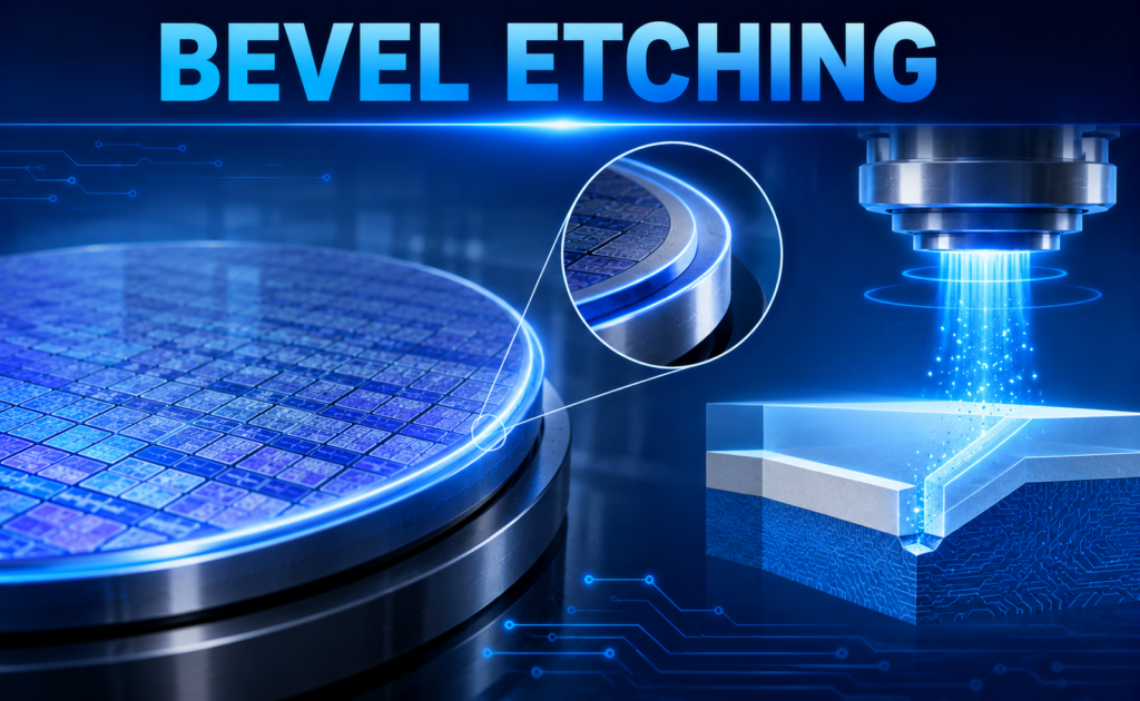
In semiconductor manufacturing, every stage of fabrication demands exceptional precision to ensure high device performance and manufacturing yield. While much attention is given to the active circuitry located at the center of the wafer, the wafer edge also plays a crucial role in maintaining process stability and preventing contamination. Material accumulation around the wafer edge […]
Wafer Grinding: Enabling Ultra-Thin Semiconductor Devices Through Precision Backside Processing
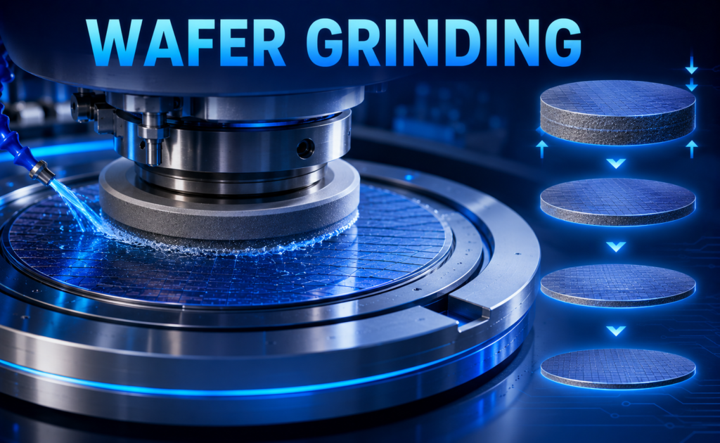
As semiconductor devices become smaller, faster, and more power-efficient, advanced packaging technologies such as 3D ICs, High-Bandwidth Memory (HBM), chiplets, and Flip Chip require increasingly thinner silicon wafers. However, standard silicon wafers are initially manufactured with sufficient thickness to withstand the numerous fabrication processes carried out during front-end manufacturing. Before packaging, these wafers must be […]
Phase Shift Mask (PSM): Enhancing Resolution in Advanced Semiconductor Lithography
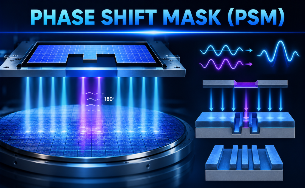
As semiconductor technology continues to scale toward 3 nm, 2 nm, and future process nodes, manufacturing extremely fine circuit features has become increasingly challenging. Conventional photolithography faces optical resolution limits, making it difficult to print densely packed transistor structures with high accuracy. To overcome these challenges, the semiconductor industry has developed innovative resolution enhancement techniques […]
Multi-Beam Lithography: Revolutionizing Next-Generation Semiconductor Patterning
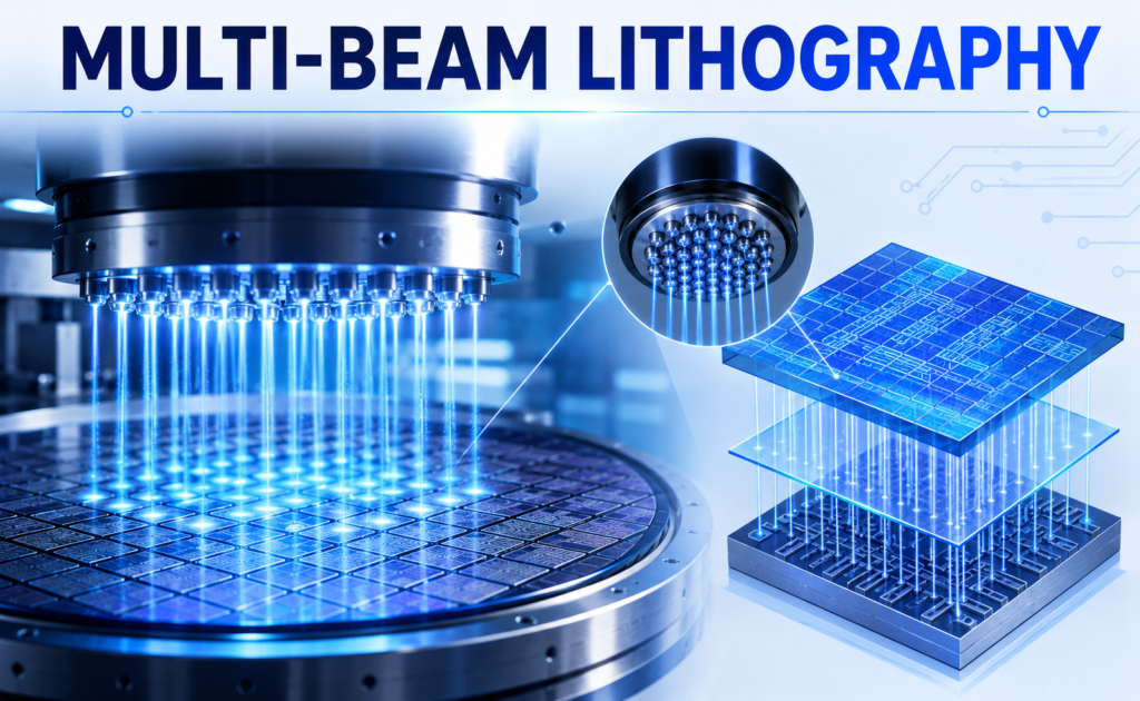
As semiconductor technology advances toward 2 nm, 1.4 nm, and future process nodes, the demand for higher transistor density and finer circuit features continues to grow. Traditional lithography methods face increasing challenges in balancing resolution, throughput, and manufacturing cost. At the same time, semiconductor manufacturers require faster mask writing and more precise pattern generation to […]
Storage Class Memory (SCM): Bridging the Gap Between Memory and Storage
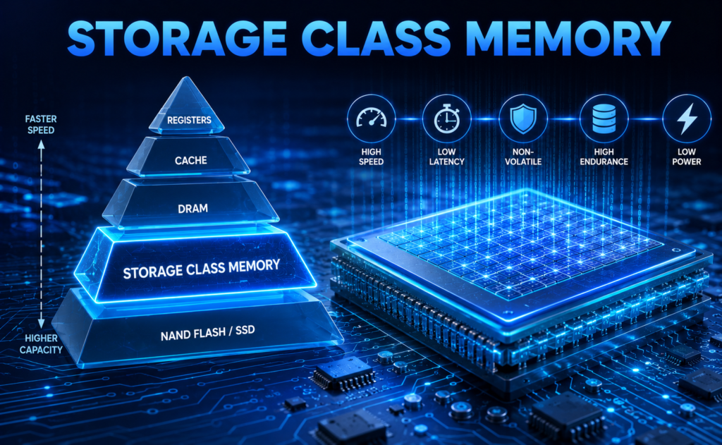
The rapid growth of artificial intelligence (AI), cloud computing, high-performance computing (HPC), and data-intensive applications has created an increasing demand for memory technologies that offer both high speed and large storage capacity. Traditional memory technologies such as DRAM provide exceptional performance but lose data when power is removed, while NAND Flash offers non-volatile storage but […]
Flip Chip Technology: Powering High-Performance Semiconductor Packaging
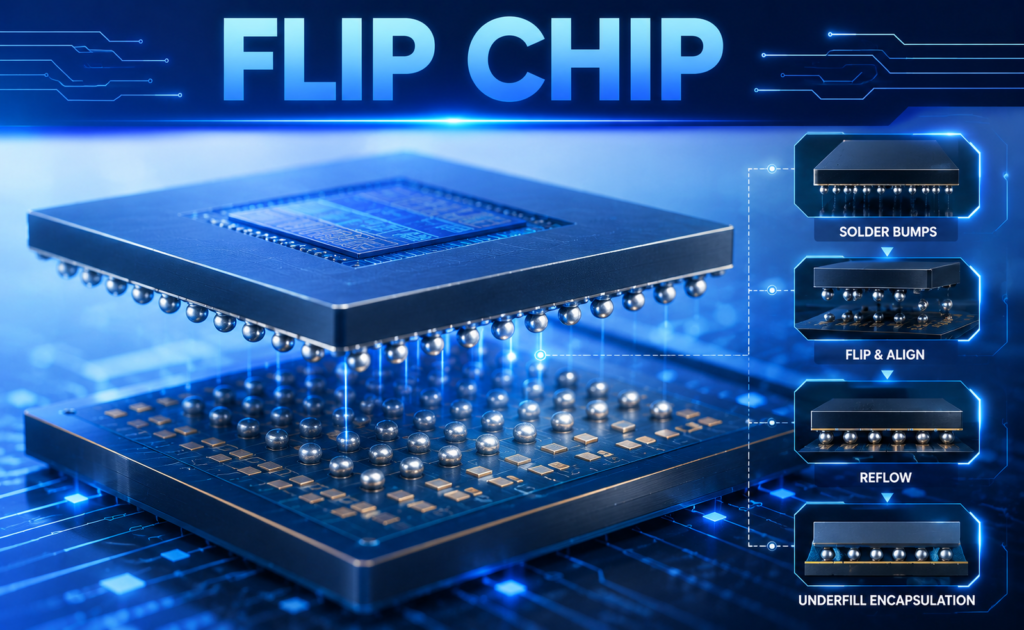
As semiconductor devices continue to evolve to meet the demands of artificial intelligence (AI), high-performance computing (HPC), 5G/6G communications, automotive electronics, and advanced consumer devices, packaging technologies have become just as important as transistor scaling. Modern processors require faster signal transmission, improved thermal performance, and higher interconnect density to deliver maximum efficiency. Flip Chip Technology […]
Wafer Dicing: The Final Precision Step in Semiconductor Manufacturing
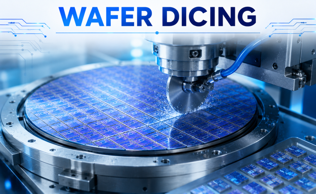
Semiconductor manufacturing involves hundreds of highly controlled fabrication processes, from transistor formation to metal interconnect creation. However, even after all circuit layers are completed, the semiconductor wafer still contains hundreds or even thousands of identical integrated circuits. Before these chips can be packaged and integrated into electronic devices, they must be separated with exceptional precision. […]
Pattern Defects: Ensuring Precision in Advanced Semiconductor Manufacturing
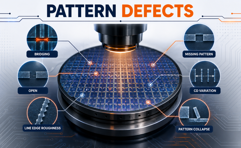
Modern semiconductor devices contain billions of transistors interconnected through nanoscale features that must be manufactured with extreme precision. As process technologies continue to advance toward 3 nm, 2 nm, and beyond, even the smallest defect in a circuit pattern can significantly impact chip functionality, manufacturing yield, and overall reliability. Pattern Defects are among the most […]
EUV Pellicle Technology: Protecting the Future of Advanced Semiconductor Lithography
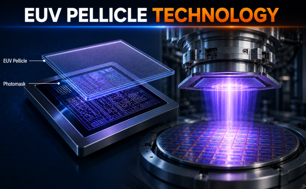
As the semiconductor industry advances toward sub-3 nm and future sub-2 nm process nodes, Extreme Ultraviolet (EUV) lithography has become the cornerstone of advanced chip manufacturing. EUV enables the fabrication of incredibly small transistor features with fewer patterning steps, allowing semiconductor manufacturers to continue scaling integrated circuits for artificial intelligence (AI), high-performance computing (HPC), mobile […]
Cryogenic Etching: Advancing Precision in Next-Generation Semiconductor Manufacturing
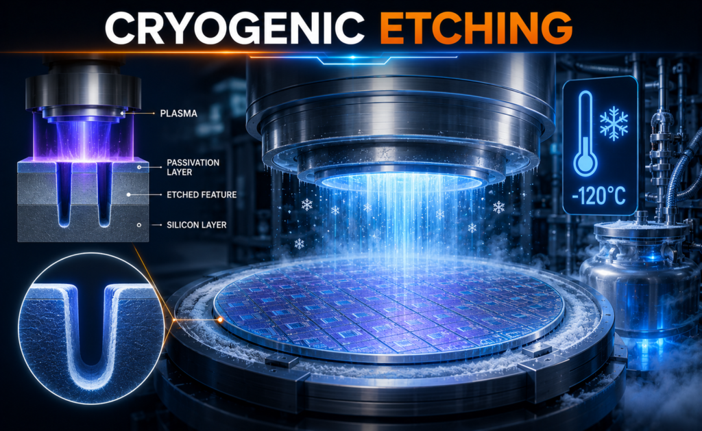
As semiconductor devices continue to scale toward sub-3 nm technology nodes, manufacturing ultra-small transistor structures with high precision has become increasingly challenging. Modern device architectures such as FinFETs, Gate-All-Around (GAA) transistors, 3D NAND, and advanced MEMS require etching processes capable of producing extremely deep, narrow, and smooth features while minimizing defects. What is Cryogenic Etching? […]