

CBRAM (Conductive Bridging RAM): Advancing the Future of Non-Volatile Semiconductor Memory
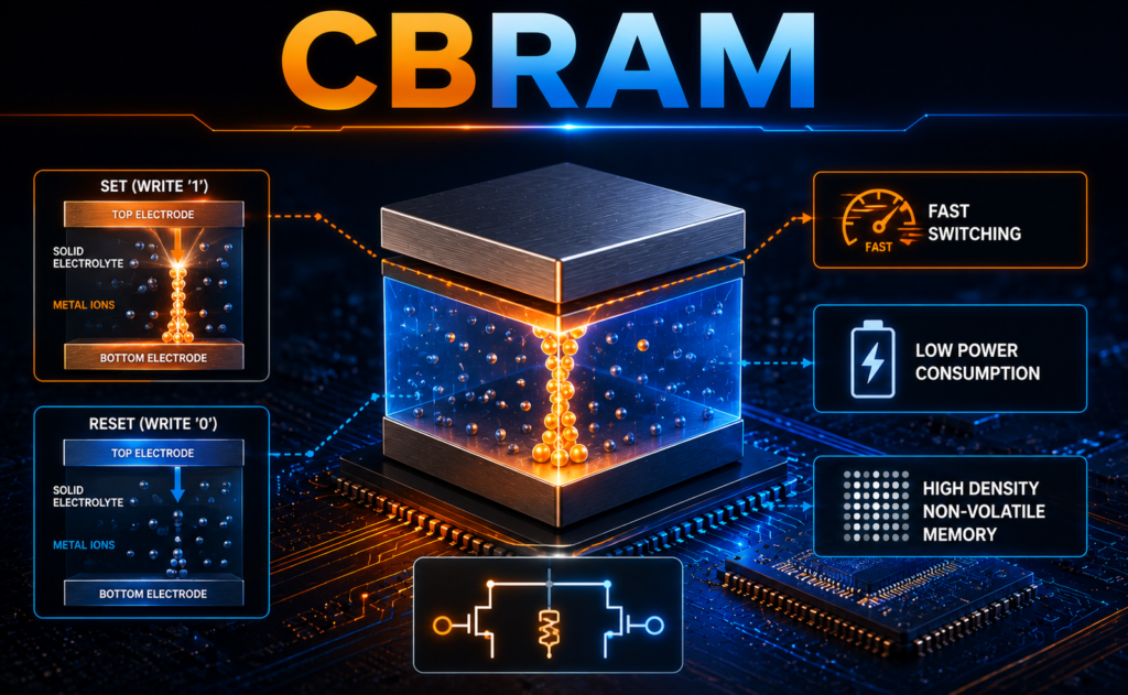
As artificial intelligence (AI), Internet of Things (IoT), edge computing, and high-performance embedded systems continue to evolve, the semiconductor industry requires memory technologies that are faster, more energy-efficient, and capable of retaining data without continuous power. Conductive Bridging RAM (CBRAM), also known as Conductive-Bridge Resistive Memory (CBRAM), is one of the most promising emerging non-volatile […]
Double Patterning: Enabling Advanced Semiconductor Lithography Beyond Conventional Limits
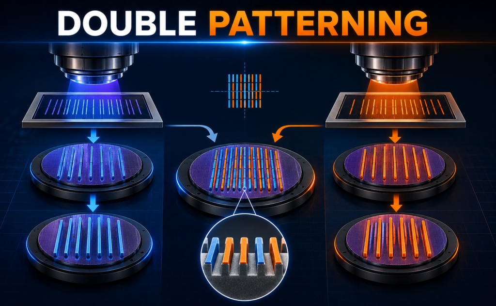
As semiconductor devices continue to shrink to advanced process nodes, manufacturing increasingly smaller transistor features has become one of the industry’s greatest challenges. Traditional photolithography techniques eventually reach physical resolution limits, making it difficult to accurately pattern extremely fine circuit features using a single exposure. Double Patterning is an advanced lithography technique developed to overcome […]
DTCO (Design-Technology Co-Optimization): Bridging Chip Design and Process Innovation
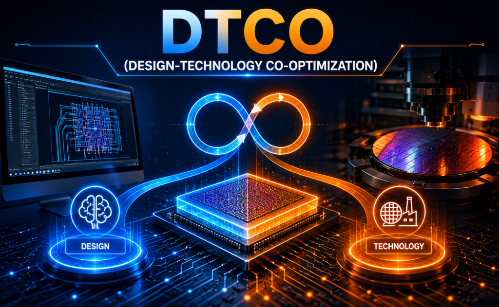
For decades, the semiconductor industry relied on transistor scaling to achieve higher performance, lower power consumption, and increased transistor density. However, as process technologies approach the limits of Moore’s Law, simply shrinking transistors is no longer sufficient to deliver the performance gains required by artificial intelligence (AI), high-performance computing (HPC), 5G/6G, and advanced mobile applications. […]
Back-End-of-Line (BEOL): The Backbone of Modern Semiconductor Interconnect Technology
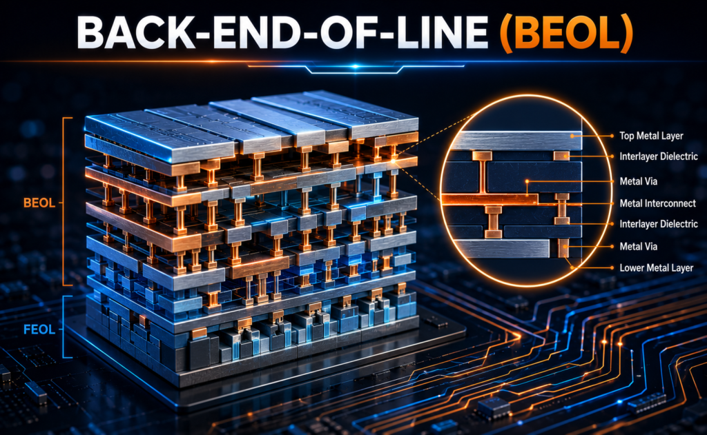
Modern semiconductor chips contain billions of transistors capable of performing trillions of operations every second. However, transistor performance alone is not enough to deliver high-speed computing. These transistors must be efficiently connected to form functional circuits that can process, store, and transfer data with minimal delay. This is where Back-End-of-Line (BEOL) technology plays a crucial […]
Glass Core Substrates: The Next Breakthrough in Advanced Semiconductor Packaging
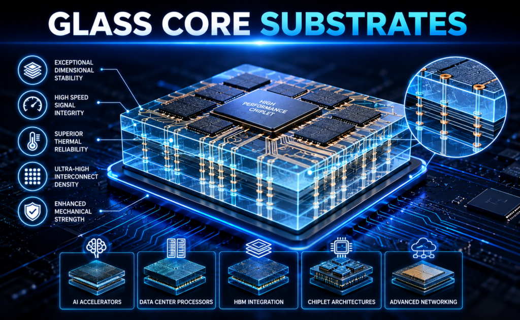
As artificial intelligence (AI), high-performance computing (HPC), advanced networking, and chiplet-based architectures continue to evolve, the semiconductor industry is facing increasing demands for higher bandwidth, greater transistor density, and improved power efficiency. While transistor innovation remains important, advancements in semiconductor packaging are becoming equally critical to overall system performance. Glass Core Substrates are emerging as […]
Monolithic 3D ICs: Revolutionizing the Next Generation of Semiconductor Integration
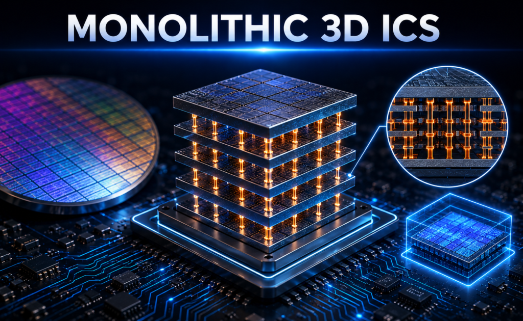
For decades, the semiconductor industry has relied on transistor scaling to improve computing performance. However, as conventional scaling approaches reach physical and economic limits, chip designers are exploring innovative integration techniques that deliver higher performance without significantly increasing chip size. Monolithic 3D Integrated Circuits (Monolithic 3D ICs) represent one of the most promising advancements in […]
Hybrid Bonding: Advancing the Future of Semiconductor Packaging
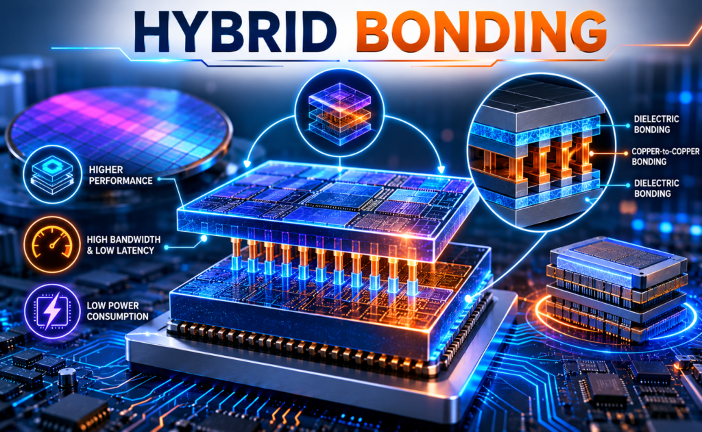
As semiconductor devices become more powerful and compact, traditional packaging technologies are reaching their physical and performance limits. Emerging applications such as artificial intelligence (AI), high-performance computing (HPC), 5G/6G communications, and data centers require faster data transfer, lower power consumption, and higher integration density than ever before. Hybrid Bonding has emerged as a breakthrough semiconductor […]
Digital Twin-Based IC Design: Transforming the Future of Semiconductor Development
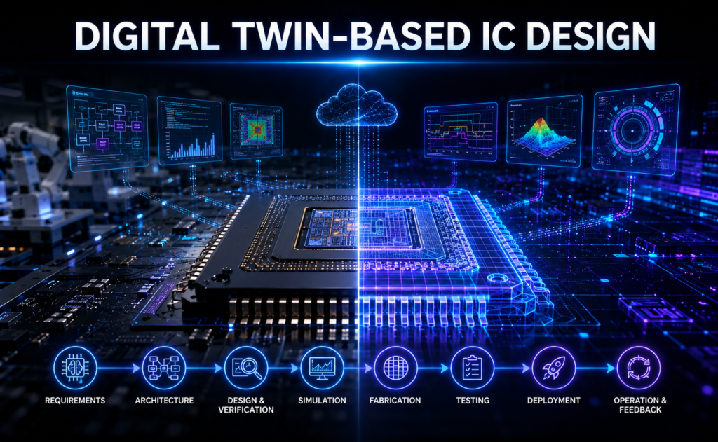
The semiconductor industry is becoming increasingly complex as integrated circuits (ICs) evolve to support artificial intelligence (AI), high-performance computing (HPC), automotive electronics, and advanced communication systems. Designing modern chips now requires billions of transistors, multiple design iterations, and extensive validation before fabrication. Digital Twin-Based IC Design is emerging as a powerful approach that creates a […]
Tensor Processing Units (TPUs): Powering the Future of AI Acceleration
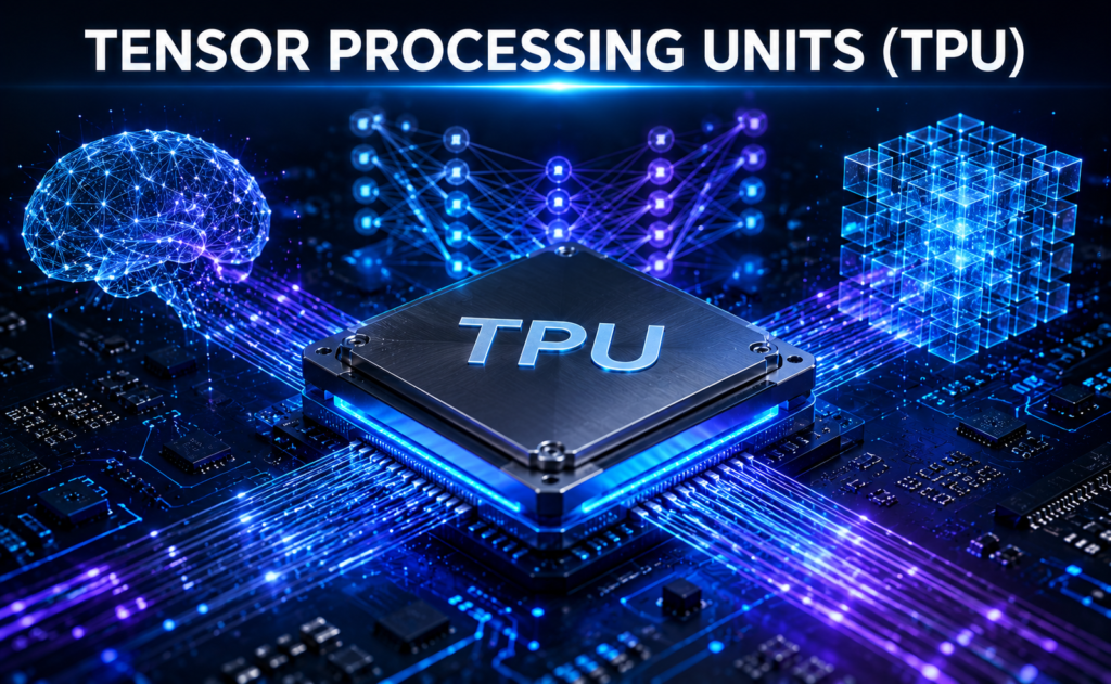
Artificial Intelligence (AI) and Machine Learning (ML) are transforming industries ranging from healthcare and finance to autonomous vehicles and cloud computing. As AI models become larger and more complex, traditional processors often struggle to deliver the required performance and energy efficiency. Tensor Processing Units (TPUs) are specialized AI accelerators designed to handle massive matrix computations […]
MRAM (Magnetoresistive RAM): Revolutionizing Next-Generation Semiconductor Memory
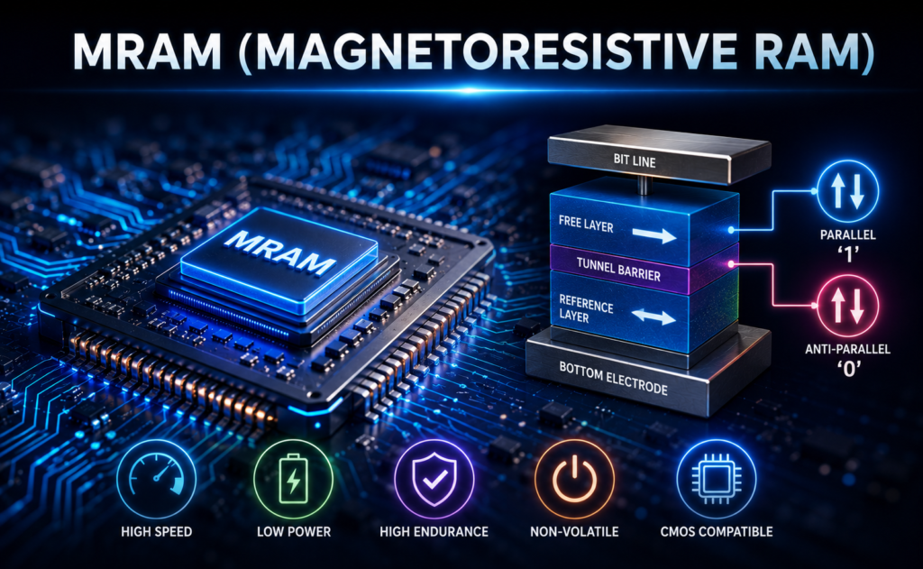
As the demand for faster computing, artificial intelligence (AI), edge devices, and energy-efficient electronics continues to grow, the semiconductor industry is exploring memory technologies that can overcome the limitations of conventional RAM and flash storage. Magnetoresistive Random Access Memory (MRAM) is one of the most promising next-generation non-volatile memory technologies. By using magnetic states instead […]