Scan Insertion, ATPG and Coverage Explained for Non-Experts
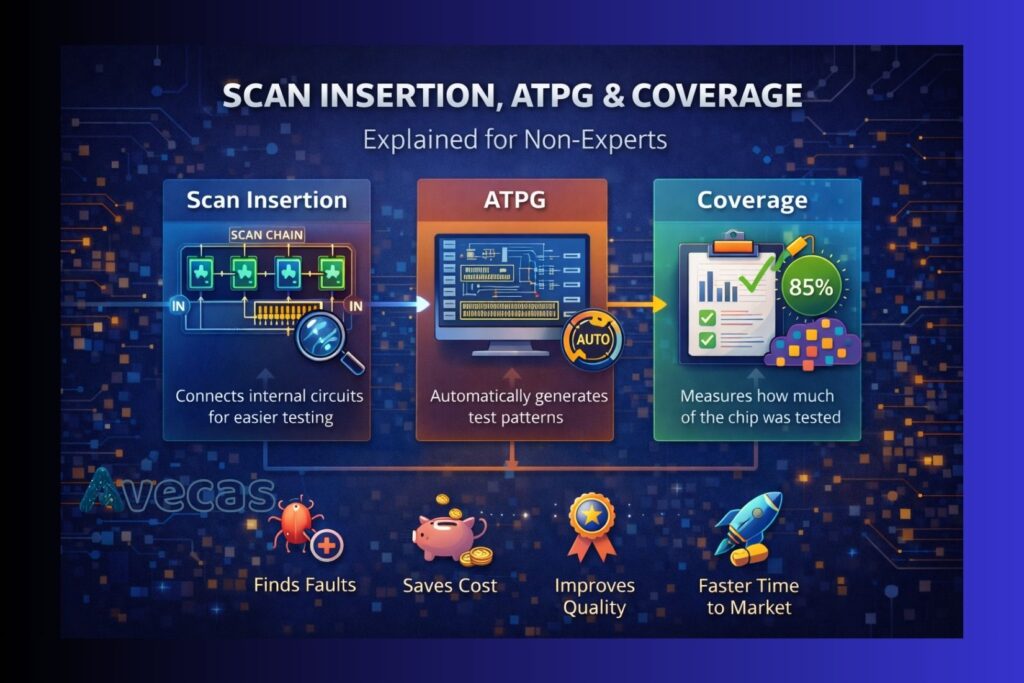
Introduction Modern semiconductor chips are extremely complex, containing millions or even billions of transistors. Ensuring that every part of a chip works correctly after manufacturing is a major challenge. This is where Design for Testability, often called DFT, becomes essential. Three key concepts in DFT are scan insertion, ATPG, and test coverage. While these terms […]
Neural Processing Units, The Future Brain for Edge AI

Introduction Artificial intelligence is rapidly moving closer to where data is generated, at the edge. From smart cameras and wearables to autonomous machines and industrial sensors, modern devices are expected to analyze data instantly without relying on constant cloud connectivity. This shift has created the need for specialized hardware, and that is where Neural Processing […]
Smart Wearables: Designing Power-Optimized PCBs for Daily Use Devices
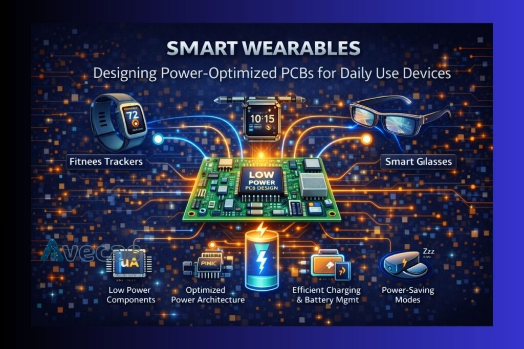
Introduction Smart wearables have become an essential part of everyday life. From fitness trackers and smartwatches to medical monitoring devices and smart glasses, users expect wearables to be lightweight, reliable, and capable of lasting all day or longer on a single charge. Behind this user experience lies a critical engineering challenge, power-optimized PCB design. Designing […]
Signal Conditioning for IoT Sensors, Techniques and Best Practices
Introduction In the world of IoT, sensors are the starting point for real world data collection. Whether monitoring temperature, motion, pressure or environmental conditions, sensor outputs are often raw signals that cannot be used directly by microcontrollers or data systems. Signal conditioning prepares these raw signals for accurate processing, increasing precision, reliability and overall performance […]
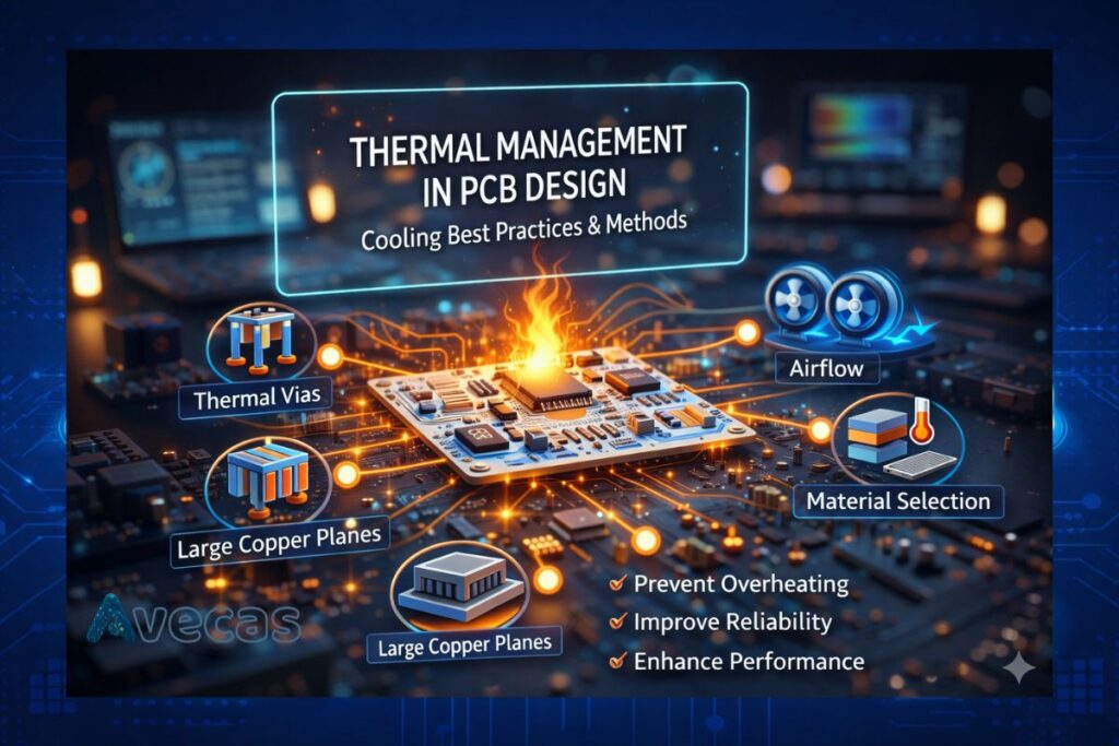
Thermal Management in PCB Design, Best Practices, Cooling Techniques, and Why It Matters
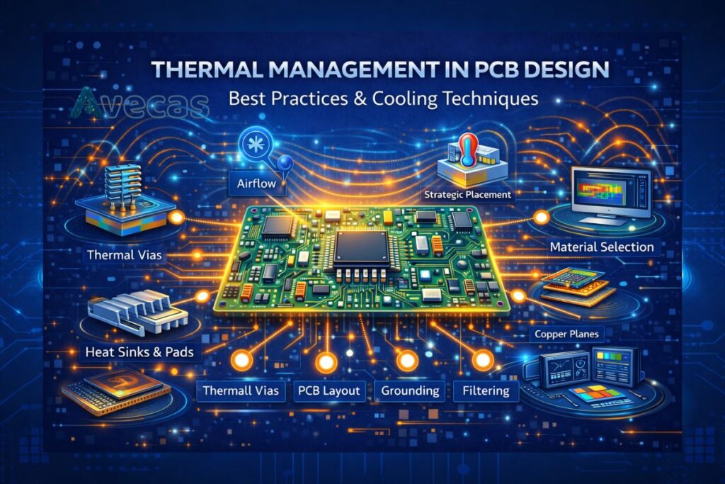
Introduction In modern electronics, managing heat is essential for reliability, performance and product longevity. As circuits become more powerful and compact, excessive heat can lead to component failure, electrical instability or reduced lifespan of devices. Thermal management in PCB design focuses on controlling heat generation and dissipation in printed circuit boards, so systems remain efficient […]
Ultimate Guide to IoT Sensors: Types, Working & Real-World Applications
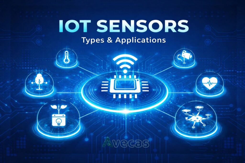
Introduction The Internet of Things (IoT) is transforming how devices interact with the physical world. At the heart of every connected system lies a crucial component, IoT sensors. These tiny electronic devices collect real-world information and transmit it to computers or cloud platforms, enabling automation, real-time monitoring, and smarter decision-making. Whether it’s smart homes, industrial […]
Custom Electronics Design: Benefits, Process & Applications
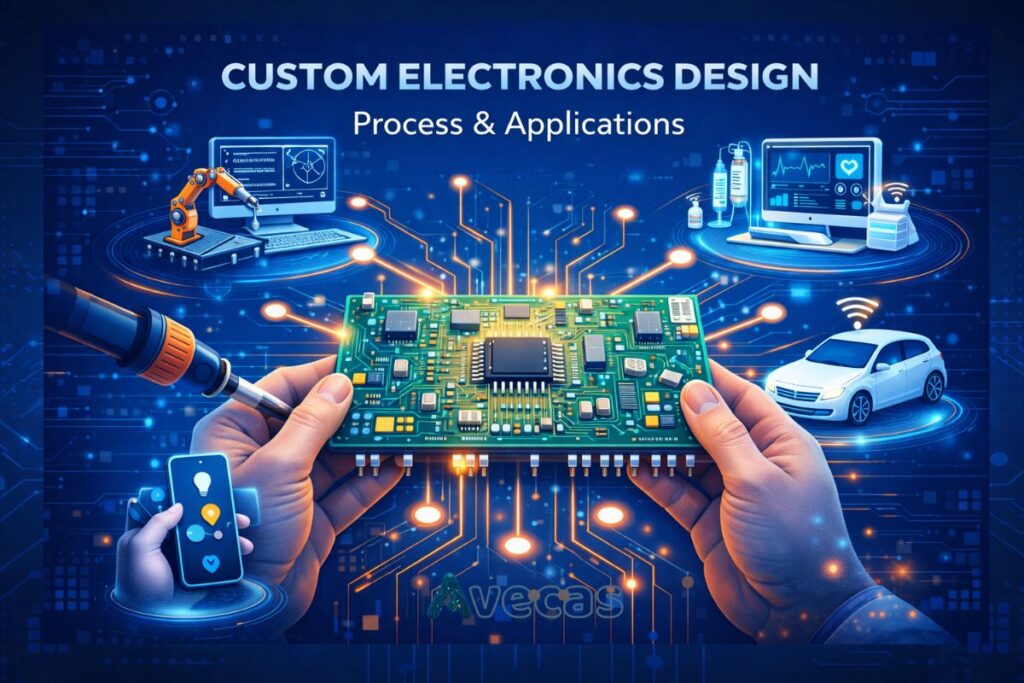
Introduction In today’s technology-driven world, off-the-shelf solutions often fall short when innovation, efficiency, or differentiation is key. That’s where custom electronics design comes in, creating tailor-made electronic systems that precisely match product specifications and business goals. Whether you’re building smart devices, industrial controllers, or IoT hardware, custom electronics designs unlock better performance, lower long-term costs, […]
VLSI Design Services in Silicon Valley, California: Powering Next-Gen Chip Innovation
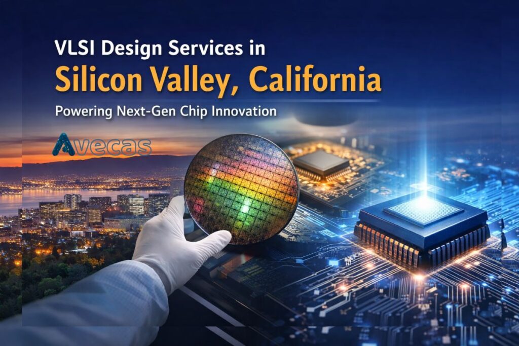
Silicon Valley, California, remains the global epicenter of semiconductor innovation. From fabless startups to multinational chipmakers, companies in this region continuously push the boundaries of performance, power efficiency, and time-to-market. As chip complexity increases across domains such as AI, automotive, data centers, and IoT, the demand for reliable and scalable VLSI design services in Silicon […]
VLSI Design Services in Hillsboro, Oregon for High-Performance Silicon

Hillsboro, Oregon is one of the most influential semiconductor hubs in the United States, known for its strong focus on advanced silicon development, manufacturing excellence, and high-performance computing innovation. The region hosts a dense ecosystem of semiconductor design centers, fabs, and R&D facilities driving next-generation processors, data center silicon, and AI-enabled platforms. As chip architectures […]
Physical Design & DFT Services for Semiconductor Firms in Chandler, Arizona
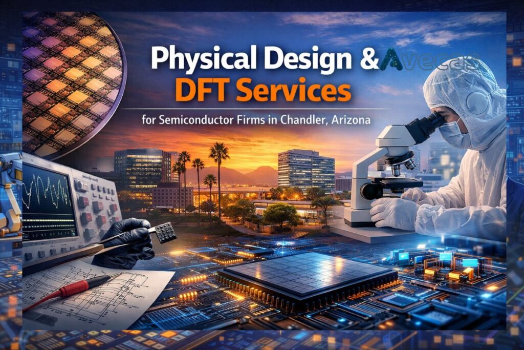
Chandler, Arizona has established itself as a strategic hub in the US semiconductor manufacturing and design ecosystem. With the presence of leading semiconductor companies, fabs, and advanced manufacturing facilities, the region plays a critical role in delivering high-volume, high-reliability silicon for global markets. As chip complexity increases, semiconductor firms in Chandler are placing greater emphasis […]