AI Assisted RTL to GDS Flow How Machine Learning is Reducing Time to Market

The semiconductor industry is under constant pressure to deliver faster, smaller, and more efficient chips. With increasing design complexity and shrinking process nodes, traditional design methodologies are struggling to keep up. This is where AI assisted RTL to GDS flow is making a significant difference. By integrating machine learning into the chip design process, companies […]
The Rise of mmWave Technology in Automobiles for High Speed Wireless Connectivity

The automotive industry is going through a major transformation driven by connectivity, automation, and intelligent systems. One of the key technologies accelerating this shift is mmWave technology. As vehicles become more connected and data driven, the need for faster and more reliable wireless communication is growing rapidly. This is where mmWave technology is making a […]
Hardware as the First Line of Defense: The Rise of Security-Aware Chip Design

For decades, the tech industry operated under a dangerous assumption: that the hardware was a trusted, neutral platform and that security was a “software problem.” We focused on firewalls, encryption algorithms, and patches. But as we move through 2026, the reality has changed. Cyber threats have migrated downstream, targeting the very transistors and gates that […]
The Speed of Light on Silicon : Unlocking 38 Tbps with Photon Driven ICs

For decades, we have relied on copper traces to move data between the cores, memory, and accelerators that power our world. But as we push into the era of massive AI clusters and hyperscale data centers in 2026, we are hitting a physical wall. Copper interconnects are struggling with three major enemies: heat, power consumption, […]
Top Future Trends Transforming Analog and Mixed-Signal (AMS) Design

For a long time, the semiconductor industry focused almost exclusively on the digital side of the house. We chased smaller transistors and faster clock speeds, often treating analog circuits as a necessary but static interface to the real world. However, as we move through 2026, the narrative has shifted completely. We are witnessing an Analog […]
Beyond the Breakdown: Leveraging AI/ML for Predictive Maintenance in Semiconductor Fabrication

In the semiconductor world of 2026, a modern fabrication plant (fab) is arguably the most complex environment on Earth. As we push toward the 2nm and 1.4nm nodes, the equipment used in lithography, etching, and deposition has become incredibly sensitive. In this high stakes environment, the cost of “unplanned downtime” is staggering. A single hour […]
DeepSeek AI: Architecting the Next Era of High-Efficiency Artificial Intelligence

In the rapidly shifting landscape of 2026, the conversation around Artificial Intelligence has moved beyond simple scale. For years, the industry believed that the only way to achieve “frontier” intelligence was through massive compute budgets and closed-door development. However, DeepSeek AI has emerged as the primary disruptor to this narrative. By focusing on architectural elegance […]
Breaking the Monolith: The Strategic Role of Open-Source Hardware in the 2026 Semiconductor Industry

For the better part of four decades, the semiconductor industry operated behind a high wall of proprietary Intellectual Property (IP) and multi-million dollar licensing fees. If you wanted to design a chip, you had to negotiate complex contracts with a handful of dominant architecture providers. However, as we navigate the landscape of 2026, those walls […]
The Humanoid Hardware Push: Architecting the Next Gen of Physical AI Chips

For the past decade, the semiconductor industry has been locked in a race to optimize “Digital AI”—chips designed to process text, images, and code within the sterile confines of a data center. However, as we move through 2026, the frontier has shifted. We have entered the era of Physical AI, where artificial intelligence must not […]
The High-NA Era: Analyzing the First Year of 0.55 NA Lithography in Volume Manufacturing
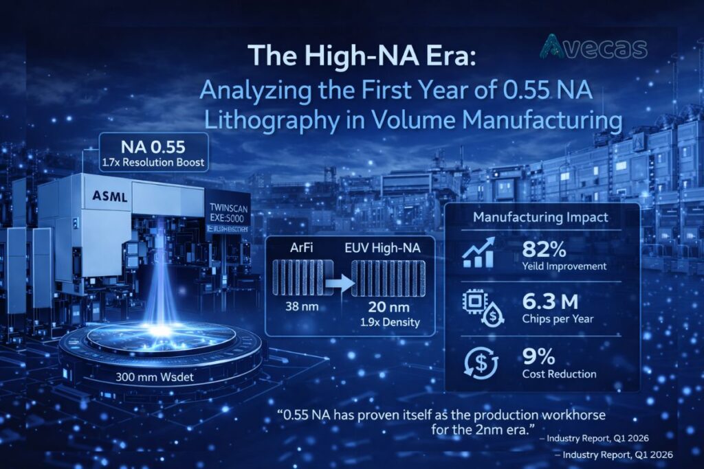
As of 2026, the semiconductor industry has crossed the threshold into the High-Numerical Aperture (High-NA) era. The deployment of the first production-grade scanners, specifically the ASML Twinscan EXE:5200, has shifted the conversation from laboratory feasibility to high-volume manufacturing (HVM) reality. For the leading-edge foundries currently pushing 2nm and 1.4nm (14A) processes, this technology is no […]