FlexICs for Item-Level Intelligence: The Missing Link in the Global AI and NFC Rollout

For decades, the semiconductor industry has been obsessed with “More Moore,” the relentless pursuit of packing more transistors into smaller, rigid blocks of silicon. While this has given us supercomputers in our pockets, it has also created a significant gap in the Internet of Things (IoT) ecosystem. Traditional silicon chips are brittle, expensive to manufacture […]
Cryogenic CMOS for Quantum Scaling: Designing the Interface Inside the Dilution Refrigerator

In the race to build a fault-tolerant quantum computer, the industry has moved beyond the era of single-qubit experiments. We are now designing systems with hundreds, and soon thousands, of qubits. However, a physical barrier has emerged that threatens to stall this progress: the “wiring crisis.” In a traditional quantum setup, every qubit is controlled […]
Software-Defined Hardware: How 2026 SoCs Adapt to AI Evolution Post-Tape-Out
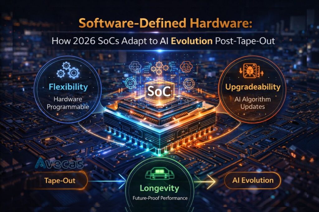
In the traditional semiconductor lifecycle, the “tape-out” was a point of no return. Once the design was sent to the foundry and the masks were created, the hardware’s logic was frozen in silicon. This rigidity worked for decades when software evolved at a predictable pace. However, in the current landscape of 2026, the artificial intelligence […]
The Vertical Revolution: Why Backside Power Delivery is the Defining Shift for 2nm Silicon

For more than half a century, the architectural blueprint of the integrated circuit followed a singular, logical path. Transistors were built on the silicon substrate, and then layers of metal wiring were built on top of them to handle both data signals and power delivery. This “frontside” approach served the industry well until we reached […]
The Rise of LAMs on Silicon: Moving Beyond Thinking to Doing with VLA Models
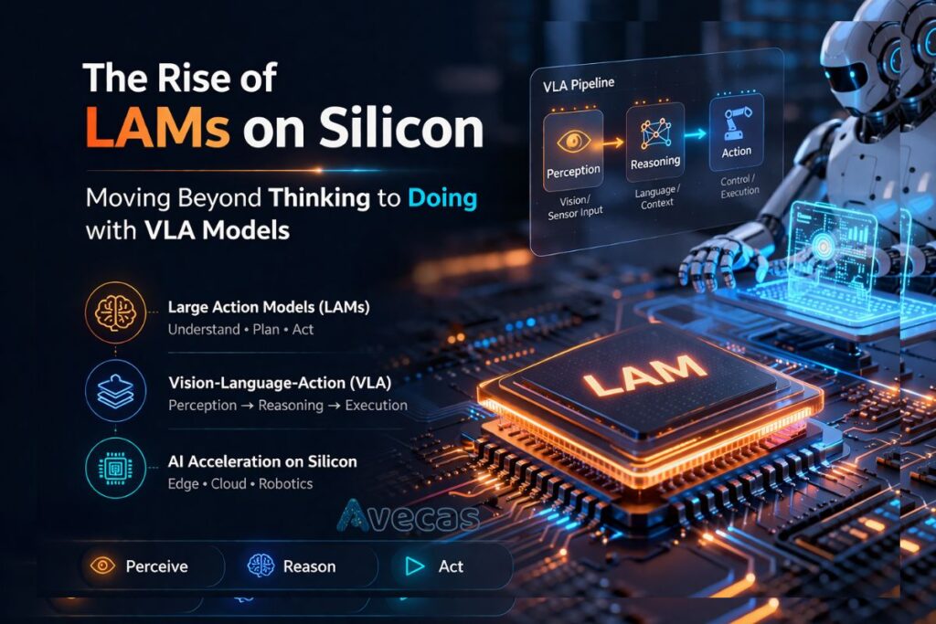
For the past several years, the semiconductor industry has been locked in a race to optimize for Large Language Models (LLMs). We built specialized accelerators designed to predict the next word in a sentence, focusing on massive memory bandwidth and high-throughput matrix multiplication. However, as we move through 2026, a new frontier has emerged that […]
The Power Transition: How GaN and SiC are Driving the 2026 EV Surge and Grid Modernization
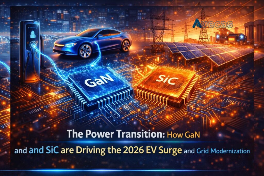
For decades, the semiconductor industry was synonymous with silicon. It was the reliable, abundant material that powered everything from the first microprocessors to the modern cloud. However, as we move through 2026, the physical limitations of traditional silicon have become a significant bottleneck for the two most critical transitions of our time: the mass electrification […]
The RISC-V Surge: Why Open-Source ISA is Becoming a Mainstream Alternative for Custom AI Silicon

For decades, the semiconductor instruction set architecture (ISA) landscape was a rigid duopoly. If you were building a high-performance server or PC, you used x86. If you were building a mobile or embedded device, you licensed ARM. This model worked well for general-purpose computing, but the explosion of artificial intelligence has fundamentally changed the requirements […]
Semiconductor Sustainability 2026: How Foundries are Reclaiming 90% of Process Water
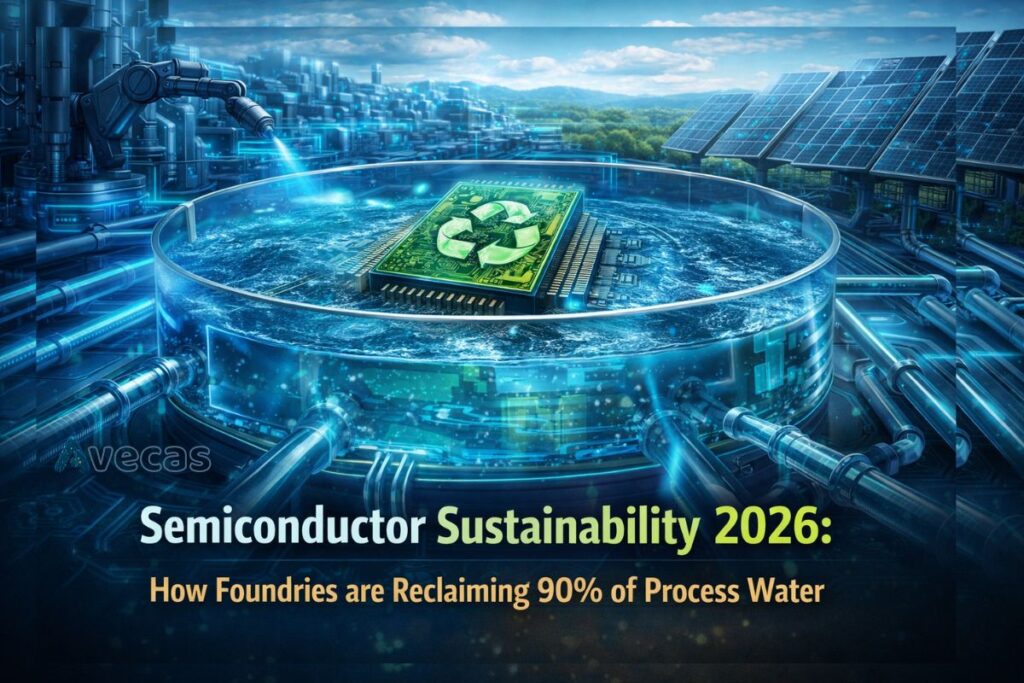
As the global demand for high-performance computing and AI hardware reaches unprecedented levels, the environmental footprint of the semiconductor industry has come under intense scrutiny. Among the various resources required to build a chip, water is perhaps the most critical. Modern “mega-fabs” can consume millions of gallons of water every single day, placing an immense […]
Known Good Die (KGD) Strategies: Minimizing Scrappage in Complex Chiplet Assembly Ecosystems
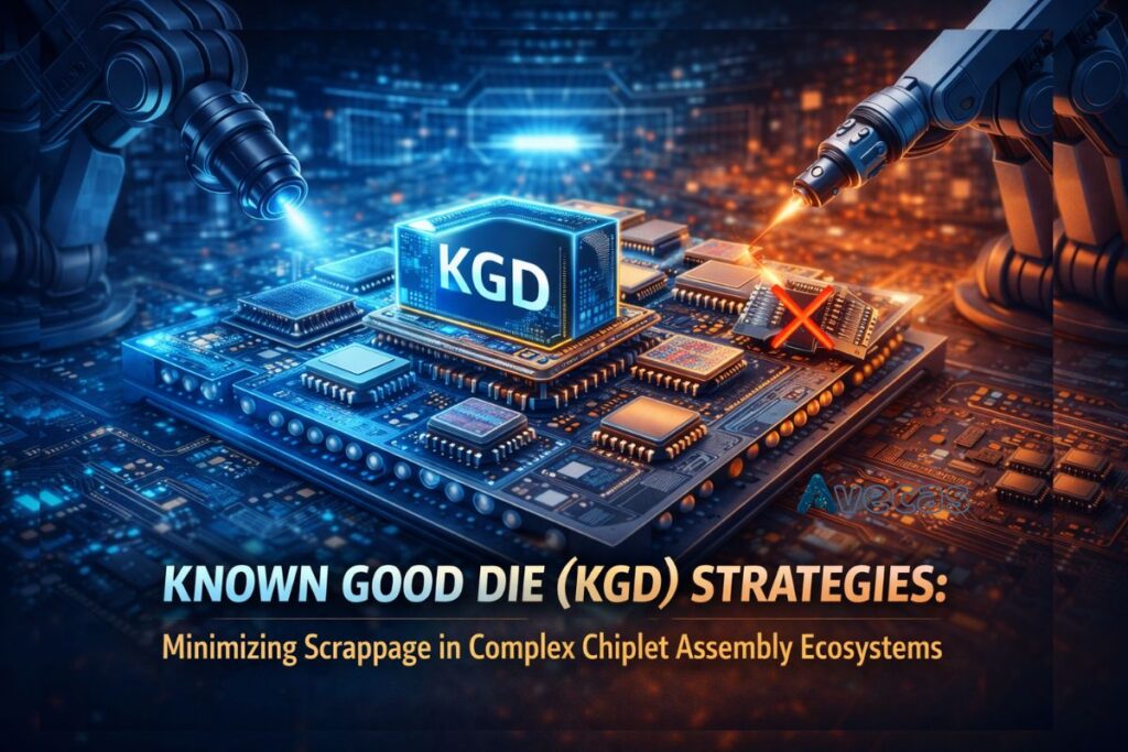
The Economic Reality of the Chiplet Era In the traditional monolithic approach to semiconductor design, a single defect on a wafer typically resulted in the loss of one individual chip. While undesirable, the financial impact was manageable and well-understood. However, as the industry pivots toward complex, multi-die architectures, the math of failure has shifted dramatically. […]
Glass Substrates vs. Organic: Why the Industry is Shifting Materials for High-Speed AI Interconnects
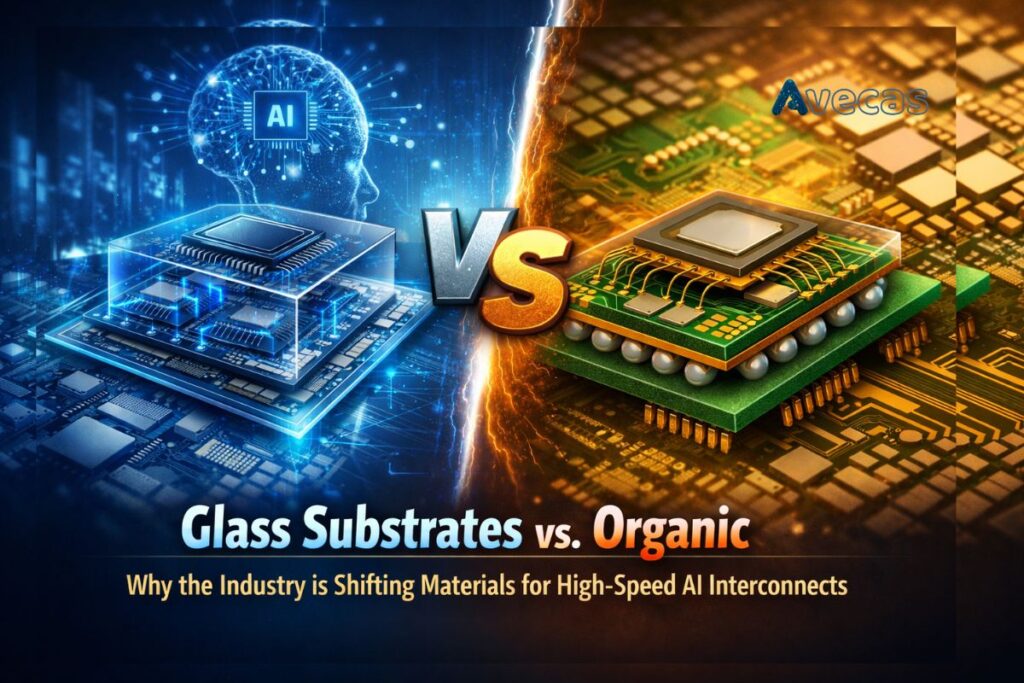
For decades, the semiconductor industry has relied on organic materials, specifically epoxy-based laminates, to serve as the foundation for chip packaging. These organic substrates have been the workhorse of the industry, providing a cost-effective and reliable way to connect silicon dies to printed circuit boards. However, as we enter the era of hyperscale AI and […]