Technical starting point
Board and FPGA targets, interfaces, throughput, latency, software responsibilities and memory bandwidth.

FPGA AND SOC INTEGRATION
Partition functions across programmable logic and processors with explicit data movement and timing contracts.
Discuss your requirements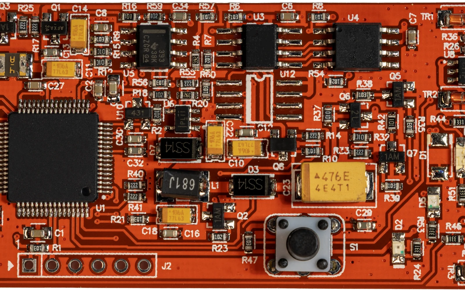
Representative photograph · Microcontroller and supporting components on a red development board.
THE ENGINEERING SCOPE
Board and FPGA targets, interfaces, throughput, latency, software responsibilities and memory bandwidth.
Timing closure, domain crossings, bus traffic, resource use and sustained throughput.
RTL, constraints, software interfaces, bitstream build instructions and integration tests.
CLIENT GUIDE
Use these technical checkpoints to make the first project review productive.
HOW WE WORK
The initial review establishes the baseline using board and FPGA targets, interfaces, throughput, latency, software responsibilities and memory bandwidth. Record gaps and dependencies before implementation.
Carry out the agreed work against the reviewed baseline. For fpga and soc integration, keep the interfaces and configuration used by this stage visible to the receiving team.
Retain the intermediate artifacts and review timing closure, domain crossings, bus traffic, resource use and sustained throughput. Investigate failures before using these results as an input to the next stage.
Package RTL, constraints, software interfaces, bitstream build instructions and integration tests. Review unresolved findings against the agreed acceptance criteria and assign ownership for follow-up.
PROJECT DECISIONS
Use these gates to agree readiness, review evidence and responsibility at each stage.
Are the starting inputs complete enough to proceed?
Board and FPGA targets, interfaces, throughput, latency, software responsibilities and memory bandwidth.
Record input revisions, missing material and who can resolve each dependency.
Has the work addressed the agreed technical objective?
Partition functions across programmable logic and processors with explicit data movement and timing contracts.
Keep the intermediate artifacts with review comments and the decisions that changed the design.
Can the result be reproduced and interpreted?
Timing closure, domain crossings, bus traffic, resource use and sustained throughput.
Capture the configuration, expected result, observed result and unresolved findings.
Can the receiving team use the delivery package?
RTL, constraints, software interfaces, bitstream build instructions and integration tests.
Review build or execution instructions, known limitations and ownership of follow-up actions.
INPUTS & OUTPUTS
The final statement of work defines the scope and acceptance criteria.
TECHNICAL DECISIONS
Partition functions across programmable logic and processors with explicit data movement and timing contracts.
The work starts from board and FPGA targets, interfaces, throughput, latency, software responsibilities and memory bandwidth. The team should identify the authoritative revision of each input and record any assumptions needed to proceed. This prevents a later result from being interpreted against a different specification or configuration.
Processor-to-logic transfers and memory contention can dominate performance even when the compute block meets its clock target.
The review centres on timing closure, domain crossings, bus traffic, resource use and sustained throughput. Each finding should identify the input revision, observed behaviour and supporting evidence. Distinguish a confirmed defect from a configuration issue, an unsupported case or an open engineering question before deciding how to resolve it.
The practical sequence is: partition compute; implement clock/reset and bus interfaces; integrate processor software; validate end-to-end performance. Intermediate reviews allow the client to resolve decisions while changes are still manageable. If an input changes, identify the affected activities and repeat the checks that depend on it.
The expected package comprises RTL, constraints, software interfaces, bitstream build instructions and integration tests. Acceptance criteria should specify what the receiving team needs to reproduce, inspect or integrate these artifacts. Include known limitations and outstanding actions in that package, rather than assuming that delivery of a file implies acceptance.
Hardware requirements should describe how signals, power and data move through the complete system. Record the intended connectors, interfaces, clock sources, reset sequence and environmental assumptions. Check component availability and the consequences of permitted substitutions. A replacement component may preserve a headline specification while changing timing, pin behaviour, thermal performance or software requirements.
Bring-up needs observable checkpoints. Establish safe supply limits and confirm rails, clocks and reset before expanding the workload. For programmable logic, keep pin assignments, clock constraints and board revisions tied to the bitstream. For a board interface, define the measurement point and probe arrangement so another engineer can reproduce the observation. Measurement equipment is part of the test setup and can influence the circuit.
Integration tests should include sustained activity and transitions between operating modes. A board that starts successfully can still fail under traffic bursts, thermal rise or simultaneous peripheral activity. Compare measured throughput with the complete data path, including memory transfers and software overhead. Document debug access, known-good configurations and the conditions needed to reproduce a failure before handing the platform to the next team.
A prototype passes a short data-transfer test but drops samples during continuous operation. Compare source rate, buffer occupancy, memory bandwidth and consumer timing while capturing power and temperature. Repeat with a controlled configuration change to distinguish a data-path bottleneck from an electrical problem. The scenario is illustrative; test limits must come from the actual product specification.
BEFORE WE BEGIN
A clear conversation is the start of a strong engineering relationship.
The starting review needs board and FPGA targets, interfaces, throughput, latency, software responsibilities and memory bandwidth. Share the current revision and known limitations so the scope reflects the actual design state.
The statement of work can define RTL, constraints, software interfaces, bitstream build instructions and integration tests. The final package should include review results and any open actions.
Processor-to-logic transfers and memory contention can dominate performance even when the compute block meets its clock target.
The first work package can be a review of the available inputs and the engineering questions that must be resolved. Agree its boundaries, access requirements and expected findings before committing to a larger implementation. A review should leave an actionable list of decisions, dependencies and next steps.
Tie each finding to the relevant revision and supporting evidence. A change should identify the affected interfaces, activities and checks. Confirm its effect on scope and delivery with the responsible owner. At handoff, distinguish closed findings, accepted limitations and open work so that a file transfer is not mistaken for technical acceptance.
PUT THE WORKFLOW IN CONTEXT
Practical reading to help prepare your project discussion. Studies are illustrative; they do not report client results.
What an embedded release should let the next engineer reproduce ↗YOUR NEXT CHAPTER STARTS HERE
Bring us your engineering challenge.
Let’s define the path from idea to implementation.