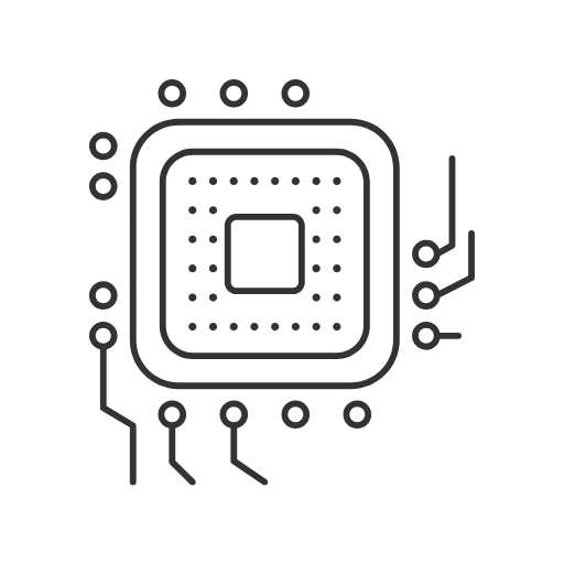


Boundary Scan, based on the IEEE 1149.1 standard (JTAG), is a critical methodology for testing interconnects on complex printed circuit boards (PCBs) without requiring extensive physical probe access. As semiconductor packages move toward high-density BGA (Ball Grid Array) and 3D stacking, traditional “bed-of-nails” testing becomes impossible. Avecas provides expert Boundary Scan and JTAG implementation services that allow for robust structural testing, in-system programming, and hardware-software debugging. Our solutions ensure that even the most densely packed designs are fully observable and controllable.
Our services provide a reliable gateway for silicon debug, hardware validation, and manufacturing test.
We design and integrate standard-compliant JTAG architectures, including Test Access Ports (TAP), Instruction Registers (IR), and Data Registers (DR). Our engineers ensure that the JTAG infrastructure is correctly partitioned to support boundary scan, internal scan, and built-in self-test (BIST) features. Standard-compliant designs ensure universal compatibility with test equipment.
Avecas implements Boundary Scan cells for all digital I/O pins, enabling the observation and control of pin states. We support various cell types to accommodate different I/O standards, ensuring that board-level “shorts” and “opens” can be detected with high precision during manufacturing. Comprehensive cell insertion maximizes board-level fault coverage.
For complex SoCs and multi-die systems, we design efficient TAP controller networks and daisy chain configurations. This allows for centralized access to multiple internal cores or external chips, simplifying the test interface and reducing the number of required physical test pins. Efficient daisy-chaining reduces PCB routing complexity and test time.
Modern designs often include high-speed AC-coupled differential signals that standard JTAG cannot test. We implement IEEE 1149.6 extensions to verify the integrity of high-speed SerDes links and other AC-coupled interconnects. AC-JTAG support ensures coverage for modern, high-speed interfaces.
We generate and rigorously validate Boundary Scan Description Language (BSDL) files. These files are essential for downstream board-level testing tools to understand the chip’s JTAG capabilities and boundary scan register sequence. Accurate BSDL files prevent delays during board-level test development.
Feel free to email us on below email address, we will be happy to answer your queries.
Minimizes the need for dedicated test points, simplifying board layout.
Your Partner for Highly Observable Designs
Deep expertise in IEEE 1149.1, 1149.6, and 1687 (IJTAG) standards.
From RTL insertion and simulation to BSDL validation and board-level support.
Proficiency with leading EDA tools for JTAG synthesis and BSDL generation.
We ensure your chip-level DFT works seamlessly with your board-level test strategy.
We support Boundary Scan and JTAG activities using industry-standard tools and proven methodologies to ensure maximum observability and board-level integrity.
Expert implementation and synthesis of Test Access Port (TAP) controllers compliant with IEEE 1149.1 standards to manage test instructions and data flow.
Creation of robust Boundary Scan Description Language (BSDL) files with automated validation to ensure seamless compatibility with board-level testers.
Designing advanced TAP linking structures for complex multi-core SoCs and daisy-chain configurations to provide unified access to internal chip logic.
Rigorous simulation of boundary scan chains to evaluate fault coverage and detect potential manufacturing defects like shorts and opens early.
designing advanced SoCs.
with specialized process needs.
demanding low-power solutions.
requiring safety-critical libraries.


A BSDL (Boundary Scan Description Language) file acts as a datasheet for the JTAG logic, telling board-level testers how to communicate with the chip to perform interconnect tests.
Yes. JTAG is widely used for software debugging, in-system programming (ISP) of flash memory, and real-time monitoring of internal signals via IJTAG (IEEE 1687).
When implemented correctly, the boundary scan cells are bypassed during normal functional mode, adding negligible load and ensuring high-speed signal integrity is maintained.
Absolutely. We specialize in designing daisy-chain architectures that allow multiple devices on a single PCB to be accessed through a single JTAG header.
Yes, we implement IJTAG to provide a scalable way to access and manage the growing number of "instruments" (like thermal sensors or BIST engines) inside modern SoCs.