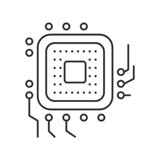


The success of a semiconductor project depends heavily on a well-defined DFT Architecture and Planning phase. As SoCs become more integrated with diverse IPs, high-speed interfaces, and complex power domains, a “one-size-fits-all” test approach is no longer viable. Avecas provides expert DFT consultancy to define the optimal test strategy early in the design cycle. We analyze your chip’s architecture to select the right mix of scan, BIST, and JTAG structures, ensuring that testability is “baked in” from day one. Our planning services minimize area overhead, optimize test time, and prevent costly late-stage design changes.
Our strategic planning ensures your design is fully testable, cost-effective, and production-ready.
We collaborate with your architects to define a custom DFT strategy based on the design’s complexity, target fault coverage, and power budget. We evaluate different test methodologies—such as hierarchical vs. flat scan—to determine the most efficient path for silicon validation. Early feasibility studies prevent architectural bottlenecks during implementation.
Avecas designs robust Test Access Mechanisms to ensure every block on the SoC can be reached and tested efficiently. We specialize in implementing standard-compliant interfaces like IEEE 1500 and IEEE 1687 (IJTAG) to manage the communication between top-level pins and internal test “instruments.”
Optimized TAM reduces the number of test pins and simplifies board-level access.
For multi-million gate designs and chiplet architectures, we implement a hierarchical DFT flow. By partitioning the design into testable “wrappers,” we enable parallel development and testing of individual blocks, which significantly reduces ATPG runtime and improves overall design predictability. Modular planning accelerates time-to-market for large-scale SoC projects.
Testing often consumes more power than functional operation. We perform early power estimation for test modes and plan for clock gating, power domain isolation, and staggered scan capture sequences to ensure the chip remains within thermal limits during the test phase. Proactive power planning protects your silicon from thermal damage during validation.
We provide comprehensive DFT specifications that serve as a blueprint for the implementation team. This includes pin-muxing strategies, clocking diagrams, scan chain estimates, and BIST configurations, ensuring a smooth transition from architecture to RTL. Clear documentation ensures alignment between design, DFT, and manufacturing teams.
Feel free to email us on below email address, we will be happy to answer your queries.
Identifying test challenges at the RTL stage avoids expensive re-spins.
Your Partner for Architecting Test-Ready Silicon
We look at the entire system—from die-level BIST to board-level JTAG—to ensure a unified strategy.
Proven experience planning for 5nm, 3nm, and advanced packaging (2.5D/3D IC).
We define architectures that work seamlessly across Siemens, Synopsys, and Cadence EDA flows.
Whether it's an ultra-low-power IoT chip or a massive AI accelerator, we tailor the plan.
We support DFT Architecture and Planning activities using industry-standard tools and proven methodologies to ensure scalable and efficient test frameworks.
Conducting comprehensive analysis at the RTL stage to identify and resolve testability bottlenecks before physical implementation begins.
Implementing standardized access mechanisms for embedded instruments and IP cores to streamline SoC-level test communication.
Developing sophisticated power models to plan for clock gating and domain isolation, ensuring silicon safety during high-toggle test cycles.
Strategically partitioning large-scale designs into modular testable units to accelerate ATPG turnaround and improve design predictability.
designing advanced SoCs.
with specialized process needs.
demanding low-power solutions.
requiring safety-critical libraries.


Ideally, DFT planning should start during the architectural phase, even before the RTL is fully written. This ensures that the clocking and power structures are designed with testability in mind.
IJTAG provides a standardized way to access internal "instruments" (like temperature sensors, BIST engines, or monitor logic) via the JTAG port. It is essential for managing the high complexity of modern SoCs.
While it adds a small amount of "wrapper" logic, the benefits in terms of reduced ATPG time, lower memory requirements, and the ability to test blocks in parallel far outweigh the minor area increase.
We utilize advanced test access standards (like IEEE 1149.1-2013 and IEEE 1838) to ensure that each chiplet can be verified independently and as part of the integrated system.
Yes. We often act as consultants, providing a complete DFT Architecture Specification that your internal design team can use to implement the DFT structures correctly.