The RISC-V Surge: Why Open-Source ISA is Becoming a Mainstream Alternative for Custom AI Silicon
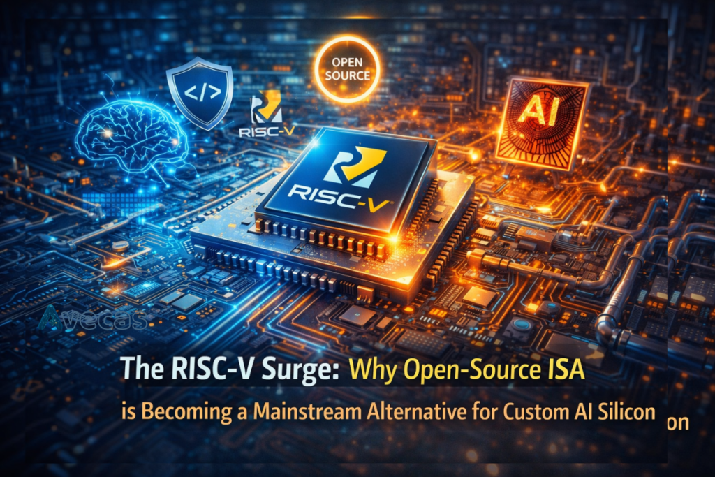
For decades, the semiconductor instruction set architecture (ISA) landscape was a rigid duopoly. If you were building a high-performance server or PC, you used x86. If you were building a mobile or embedded device, you licensed ARM. This model worked well for general-purpose computing, but the explosion of artificial intelligence has fundamentally changed the requirements […]
Semiconductor Sustainability 2026: How Foundries are Reclaiming 90% of Process Water
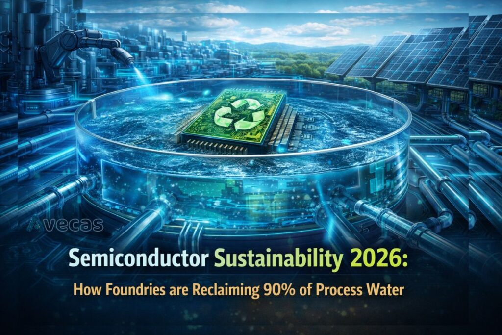
As the global demand for high-performance computing and AI hardware reaches unprecedented levels, the environmental footprint of the semiconductor industry has come under intense scrutiny. Among the various resources required to build a chip, water is perhaps the most critical. Modern “mega-fabs” can consume millions of gallons of water every single day, placing an immense […]
Known Good Die (KGD) Strategies: Minimizing Scrappage in Complex Chiplet Assembly Ecosystems
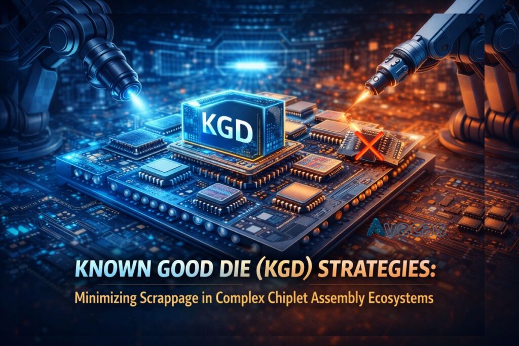
The Economic Reality of the Chiplet Era In the traditional monolithic approach to semiconductor design, a single defect on a wafer typically resulted in the loss of one individual chip. While undesirable, the financial impact was manageable and well-understood. However, as the industry pivots toward complex, multi-die architectures, the math of failure has shifted dramatically. […]
Glass Substrates vs. Organic: Why the Industry is Shifting Materials for High-Speed AI Interconnects
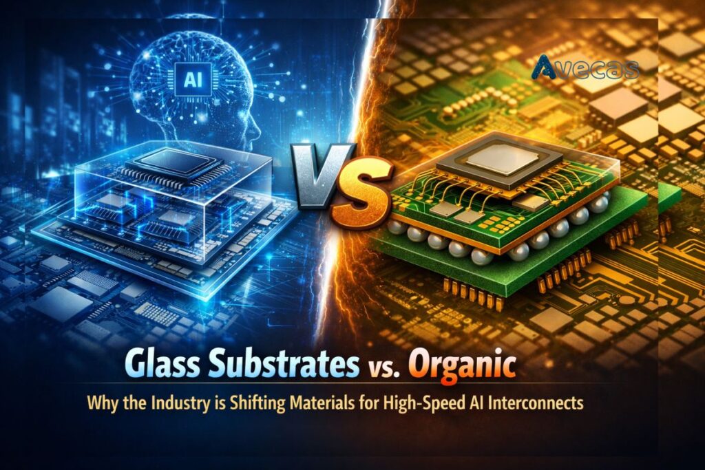
For decades, the semiconductor industry has relied on organic materials, specifically epoxy-based laminates, to serve as the foundation for chip packaging. These organic substrates have been the workhorse of the industry, providing a cost-effective and reliable way to connect silicon dies to printed circuit boards. However, as we enter the era of hyperscale AI and […]
Neuromorphic Computing: Moving Beyond Von Neumann Architectures for Brain-Inspired Silicon
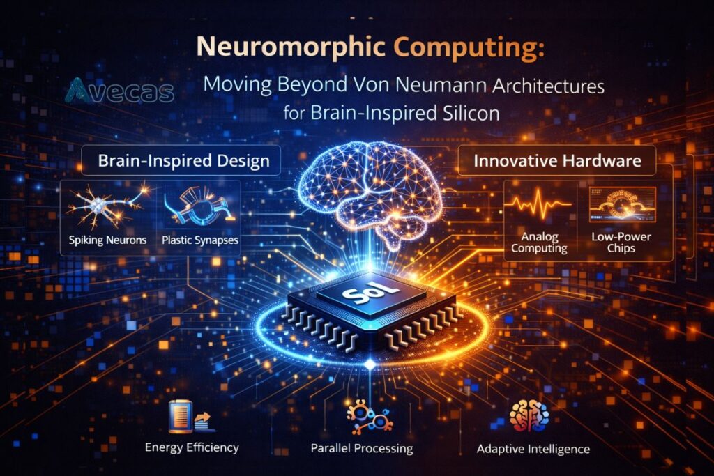
For over seventy years, the foundation of every computer—from the massive mainframes of the 1950s to the smartphone in your pocket has remained virtually unchanged. We have lived in the era of the Von Neumann architecture, a design where the processing unit and memory are physically separate entities. While this model has powered the digital […]
The Intelligence Inflection: How Generative AI is Revolutionizing VLSI Design and Verification
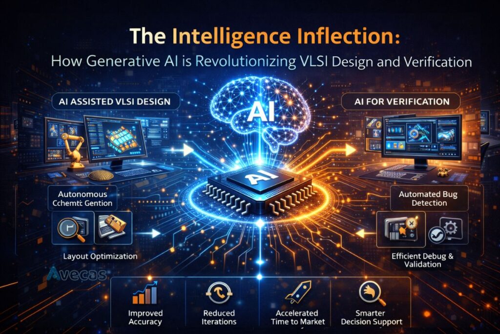
The semiconductor industry is currently navigating its most significant paradigm shift since the introduction of Logic Synthesis in the 1980s. As we push the boundaries of 2nm and 3nm process nodes, the sheer complexity of modern Integrated Circuits (ICs) has outpaced human-centric design methodologies. We are no longer just designing chips; we are managing massive, […]
The Rise of Chiplets: Redefining Semiconductor Manufacturing and Design Services
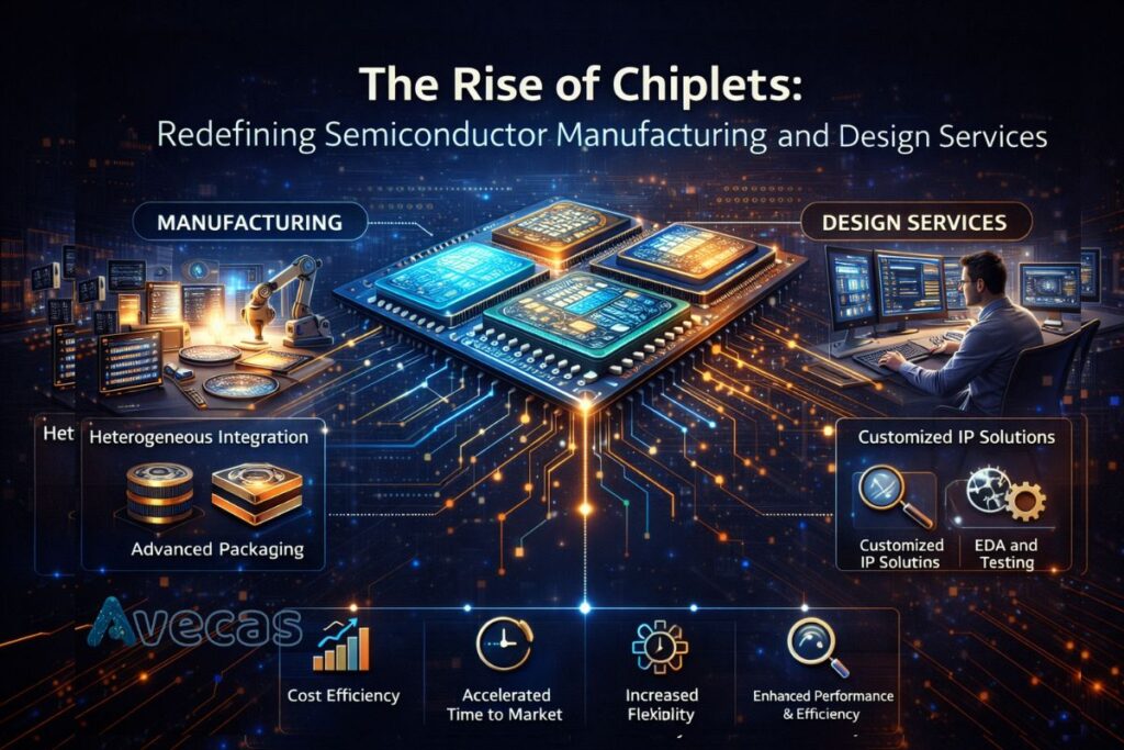
For decades, the semiconductor industry followed a predictable path: make transistors smaller to pack more power onto a single piece of silicon. However, as we approach the physical limits of atomic-scale manufacturing, the “monolithic” approach, where every component is on one large die is becoming prohibitively expensive and technically challenging. Enter the era of Chiplets […]
The Future of Backend Semiconductor Engineering in the AI Era
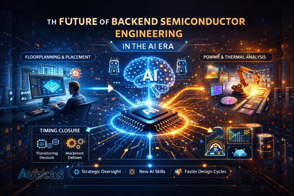
Introduction Backend semiconductor engineering has always been one of the most demanding phases of chip development. As designs move to advanced technology nodes and system complexity grows, backend teams face increasing pressure to deliver high performance, low power, and manufacturable silicon within shorter timelines. With artificial intelligence becoming deeply embedded into electronic design automation and […]
Scan Insertion, ATPG and Coverage Explained for Non-Experts
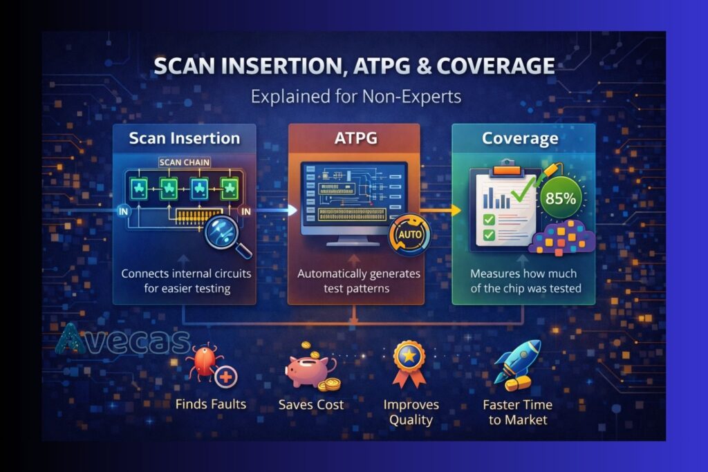
Introduction Modern semiconductor chips are extremely complex, containing millions or even billions of transistors. Ensuring that every part of a chip works correctly after manufacturing is a major challenge. This is where Design for Testability, often called DFT, becomes essential. Three key concepts in DFT are scan insertion, ATPG, and test coverage. While these terms […]
Neural Processing Units, The Future Brain for Edge AI
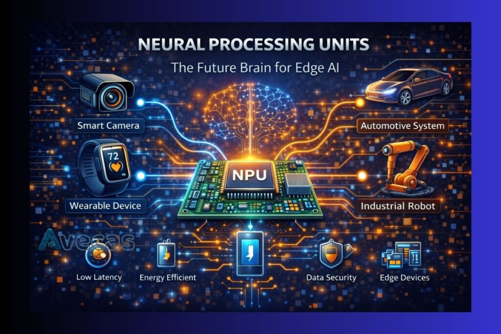
Introduction Artificial intelligence is rapidly moving closer to where data is generated, at the edge. From smart cameras and wearables to autonomous machines and industrial sensors, modern devices are expected to analyze data instantly without relying on constant cloud connectivity. This shift has created the need for specialized hardware, and that is where Neural Processing […]