01
Discover
Review the specification, technology dependencies, available IP, tool access, schedule, and delivery risks.

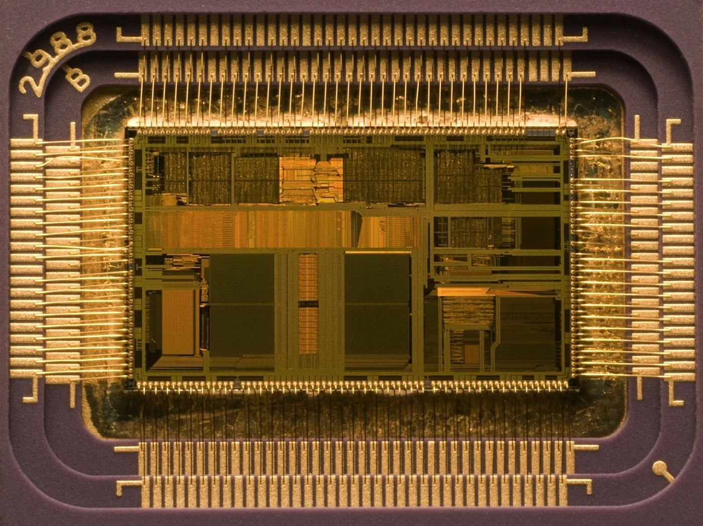
SEMICONDUCTOR & EMBEDDED ENGINEERING
RTL, verification, physical design, DFT, custom IP, and embedded systems. Work with Avecas on a specialist design task or a coordinated turnkey programme.
THE AVECAS APPROACH
A chip programme involves different disciplines, each with its own inputs and handoffs. Avecas brings IC design, EDA workflows, and embedded engineering together around your specification, tool environment, and delivery schedule.
Meet your engineering partnerWHAT WE BUILD
A connected set of capabilities, from the chip at the heart of your product to the software and systems around it.
Architecture, RTL, verification, physical design, and test engineering.
Explore solutions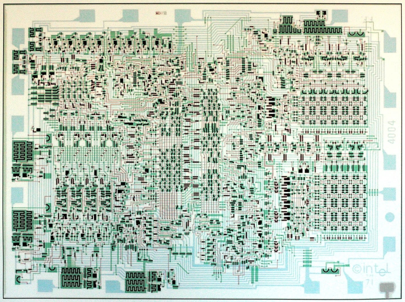
Hardware, firmware, FPGA, and the software that connects your system.
Explore solutions
Applications, engineering automation, cloud, and data workflows.
Explore solutions
Explore project engineering, technical collaboration, and specialist support.
Explore solutions01 / ENGINEERING CAPABILITIES
From the first architecture decision to the final integration detail, find the expertise your design needs.
Every block has a purpose.
Every interface matters.
Turn system requirements into clear microarchitecture, synthesizable RTL, and an integration plan.
Explore RTL & architectureBuild confidence with verification planning, simulation, coverage analysis, and formal methods.
Explore Design verificationConnect implementation decisions to timing, power, area, and physical signoff requirements.
Explore Physical designPlan test architecture, scan integration, ATPG, and the handoff to production test.
Explore Design for testSupport analog layout, integration, and verification across the agreed process and design rules.
Explore Analog & mixed signalBring hardware and software together through prototyping, firmware, and system validation.
Explore Embedded & FPGA02 / TURNKEY IC DESIGN
Connect design disciplines around a defined scope. Make the interfaces, milestones, and acceptance evidence clear from the start.
Explore turnkey projectsReview the specification, technology dependencies, available IP, tool access, schedule, and delivery risks.
Set ownership, interfaces, review milestones, and measurable acceptance criteria.
Work through implementation and verification with regular technical reviews and visible issue tracking.
Review the deliverables against the acceptance plan and agree the next stage of integration or validation.
03 / IP, DEVELOPMENT & RESEARCH
Explore custom IP engineering, internal development, and research collaboration. Start with the problem worth solving.
BUILT AROUND YOUR SYSTEM
From a block specification to documented integration. Designed around the interfaces that matter.
Explore IP engineering ↗IN-HOUSE DEVELOPMENT
Explore development opportunities and technical collaboration.
Explore development ↗RESEARCH & INNOVATION
Research collaboration, disclosure, and intellectual property.
Explore research ↗WHY AVECAS
The strongest engineering partnerships begin with a shared understanding of the problem. Here is how we approach the work.
More about Avecas ↗Consider architecture, implementation, verification, and system integration together, with clear interfaces between disciplines.
Define the functional scope, integration requirements, reuse rights, and delivery evidence for your custom IP engagement.
Discuss reusable design collateral, verification workflows, and automation opportunities within the agreed project scope.
Agree the technical milestones, responsibilities, review points, and acceptance criteria before execution begins.
04 / ENGINEERING JOURNAL
Oct 12, 2026
As semiconductor manufacturing advances toward smaller technology nodes, creating precise nanoscale patterns has become increasingly challenging. Modern integrated circuits require extremely narrow lines, tiny…
Read article Pattern Transfer Through Ultrathin Resist in Advanced Semiconductor LithographyOct 11, 2026
Scope an IC design engagement with clear inputs, acceptance criteria, ownership, review milestones, and reproducible handoff evidence.
Read article Planning a turnkey IC design project: a practical handoff checklistOct 10, 2026
As semiconductor technology advances toward smaller transistors and increasingly complex device architectures, measuring microscopic features accurately has become essential for maintaining chip performance and…
Read article How Does CD-SEM Measure Tiny Features in Semiconductor Chips?Avecas is a fabless semiconductor and EDA services company working across IC design, custom IP, verification, physical design, DFT, and embedded engineering.
Yes. Engagements can cover a specialist work package, custom IP engineering, project coordination, or a defined turnkey scope.
Start with the specification, current design state, target technology, schedule, and required deliverables. Fabrication, IP licensing, packaging, and test responsibilities are agreed explicitly.
Use the contact page to share a non-confidential summary of the application, design stage, engineering need, and target schedule. The next step is a technical scope review.
YOUR NEXT CHAPTER STARTS HERE
Bring us your engineering challenge.
Let’s define the path from idea to implementation.