EXPLORE AVECAS
Engineering insights
Perspectives on silicon design, verification, embedded systems, and the engineering decisions behind them.
Oct 31, 2026
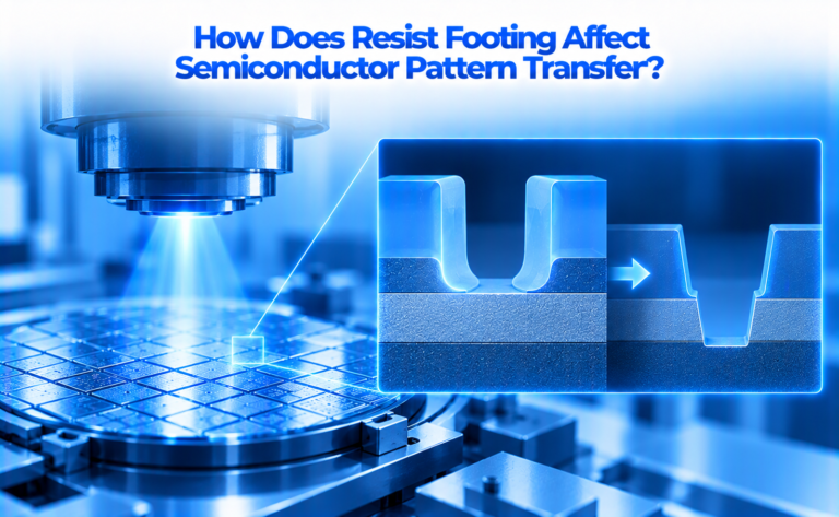
In semiconductor manufacturing, photolithography defines the tiny patterns that eventually become transistors, contacts, and interconnects on a silicon wafer. For accurate pattern formation, the…
Read article How Does Resist Footing Affect Semiconductor Pattern Transfer? ↗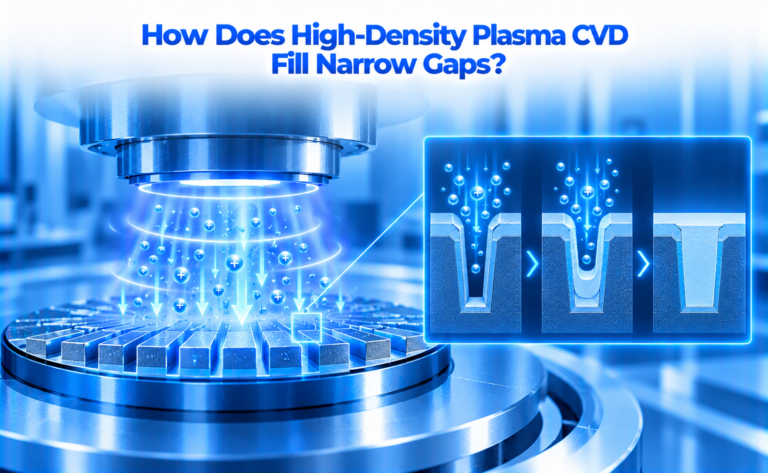
Oct 30, 2026
As semiconductor devices continue to shrink, creating reliable electrical isolation between closely spaced structures has become increasingly challenging. Advanced integrated circuits contain dense transistor…
Read article How Does High-Density Plasma CVD Fill Narrow Gaps? ↗
Oct 29, 2026
As semiconductor packages become more compact and complex, ensuring the integrity of internal material interfaces is essential for long-term reliability. Modern integrated circuits contain…
Read article Why Is Acoustic Microscopy Used to Detect Package Delamination? ↗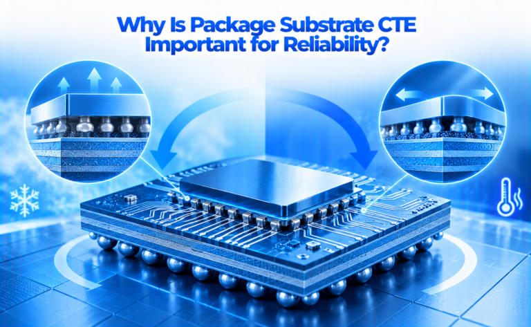
Oct 28, 2026
As semiconductor devices become more powerful and advanced, package reliability has become just as important as transistor performance. Modern processors, AI accelerators, memory devices,…
Read article Why Is Package Substrate CTE Important for Reliability? ↗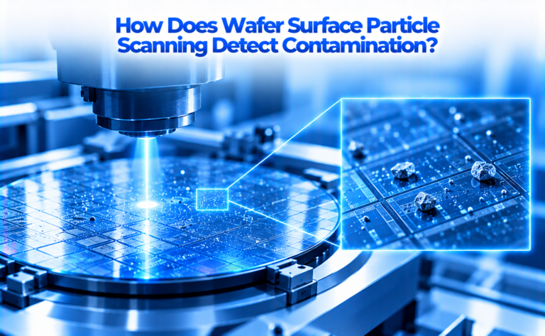
Oct 27, 2026
Semiconductor manufacturing requires extremely clean wafer surfaces because even microscopic particles can interfere with lithography, deposition, etching, and other critical fabrication processes. As transistor…
Read article How Does Wafer Surface Particle Scanning Detect Contamination? ↗
Oct 26, 2026
In semiconductor manufacturing, even small variations in transistor dimensions, threshold voltage, and interconnect characteristics can influence how quickly a chip performs its operations. Although…
Read article How Does Ring Oscillator Testing Reveal Process-Speed Variation? ↗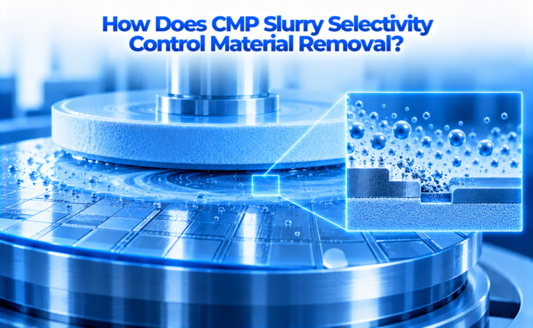
Oct 24, 2026
As semiconductor devices become smaller and more complex, achieving a flat, uniform wafer surface is essential for reliable chip manufacturing. Multiple layers of dielectric…
Read article How Does CMP Slurry Selectivity Control Material Removal? ↗
Oct 23, 2026
In semiconductor manufacturing, lithography defines the tiny patterns that eventually become transistor gates, contacts, vias, and interconnects. However, creating the intended pattern in photoresist…
Read article How Does Resist Footing Affect Semiconductor Pattern Transfer? ↗
Oct 22, 2026
NAND flash memory is a fundamental technology behind solid-state drives (SSDs), USB drives, memory cards, and many embedded storage systems. As NAND technology advances…
Read article Why Is Read Disturb a Reliability Challenge in NAND Flash? ↗
Oct 21, 2026
Plasma etching is one of the most important processes in semiconductor manufacturing, enabling engineers to create precise nanoscale patterns in silicon, dielectrics, metals, and…
Read article Why Does Etch Polymer Build Up on Chamber Walls? ↗
Oct 19, 2026
In semiconductor manufacturing, achieving a high-quality thin film requires more than selecting the right deposition material and process parameters. The condition of the wafer…
Read article Why Is Wafer Surface Hydrophobicity Important Before Deposition? ↗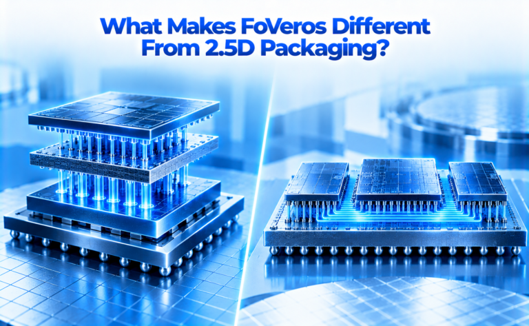
Oct 17, 2026
As semiconductor devices become more powerful, chip designers are increasingly looking beyond traditional single-die architectures to improve computing performance, energy efficiency, and integration density.…
Read article What Makes Foveros Different From 2.5D Packaging? ↗