EXPLORE AVECAS
Engineering insights
Perspectives on silicon design, verification, embedded systems, and the engineering decisions behind them.

Oct 9, 2026
As semiconductor devices become more powerful and complex, connecting multiple silicon dies with high bandwidth and low power consumption has become a major engineering…
Read article Why Are Microbumps Being Replaced by Finer-Pitch Bonding Technologies? ↗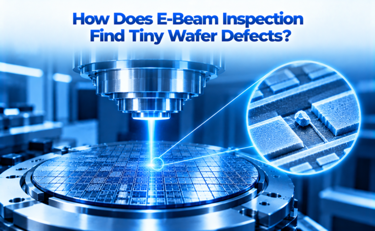
Oct 8, 2026
As semiconductor technology continues to scale, manufacturing defects that were once considered insignificant can become large enough to affect transistor performance, yield, or chip…
Read article How Does E-Beam Inspection Find Tiny Wafer Defects? ↗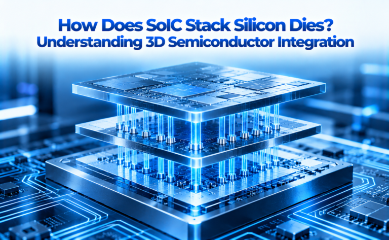
Oct 7, 2026
As semiconductor systems demand more computing power, higher bandwidth, and lower energy consumption, simply making individual transistors smaller is no longer the only path…
Read article How Does SoIC Stack Silicon Dies? Understanding 3D Semiconductor Integration ↗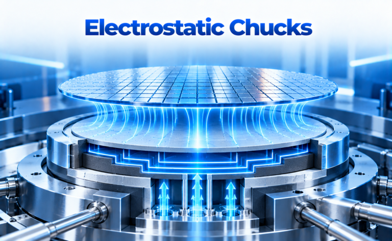
Oct 6, 2026
Inside a semiconductor fabrication chamber, a wafer must remain precisely positioned while processes such as plasma etching, deposition, ion implantation, and cleaning take place.…
Read article Electrostatic Chucks in Semiconductor Manufacturing: How ESCs Hold and Control Wafers ↗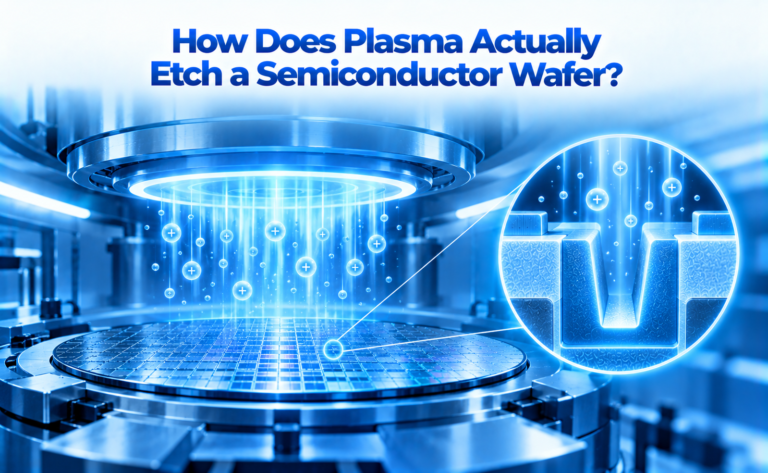
Oct 1, 2026
Modern semiconductor chips contain structures that are measured in nanometers, yet these structures must be created with remarkable precision across an entire silicon wafer.…
Read article How Does Plasma Actually Etch a Semiconductor Wafer? ↗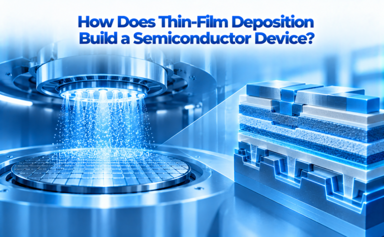
Sep 29, 2026
A modern semiconductor device is built from an intricate stack of extremely thin material layers. These layers may act as conductors, insulators, barriers, spacers,…
Read article How Does Thin-Film Deposition Build a Semiconductor Device? ↗
Sep 28, 2026
Every application running on a computer from opening a browser to running artificial intelligence software ultimately depends on one fundamental process: the CPU executing…
Read article How Does a CPU Actually Execute Instructions? ↗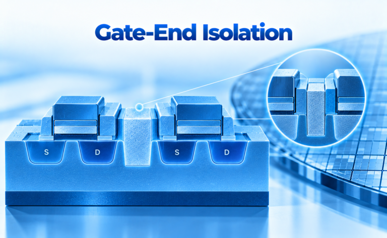
Sep 22, 2026
As semiconductor technology continues to scale, reducing transistor dimensions requires much more than shrinking the gate length. The spaces at the ends of transistor…
Read article Gate-End Isolation in Advanced CMOS: Enabling Compact and Reliable Transistor Architectures ↗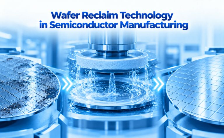
Sep 19, 2026
As semiconductor manufacturing becomes increasingly resource-intensive, wafer manufacturers are focusing not only on device performance and yield but also on material efficiency, cost optimization,…
Read article Wafer Reclaim Technology in Semiconductor Manufacturing ↗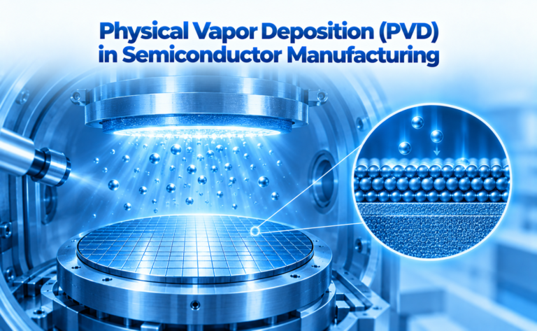
Sep 18, 2026
As semiconductor devices continue to scale, manufacturers require increasingly precise methods for depositing extremely thin and uniform material layers. These films form critical parts…
Read article Physical Vapor Deposition (PVD) in Semiconductor Manufacturing ↗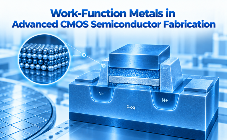
Sep 17, 2026
As CMOS technology advances toward smaller process nodes, controlling the electrical behavior of the transistor gate becomes increasingly important. Traditional polysilicon gates face limitations…
Read article Work-Function Metals in Advanced CMOS Semiconductor Fabrication ↗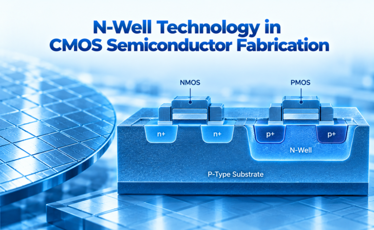
Sep 16, 2026
CMOS technology is the foundation of modern digital integrated circuits, powering processors, memory devices, microcontrollers, sensors, and a wide range of electronic systems. A…
Read article N-Well Technology in CMOS Semiconductor Fabrication ↗