

CMOS technology is the foundation of modern digital integrated circuits, powering processors, memory devices, microcontrollers, sensors, and a wide range of electronic systems. A key requirement in CMOS fabrication is the ability to integrate both NMOS and PMOS transistors on the same silicon substrate.
N-Well Technology is one of the fundamental CMOS fabrication approaches used to create the required regions for PMOS transistor formation. By forming an n-type well inside a p-type silicon substrate, the process provides an appropriate body region for PMOS devices while allowing NMOS devices to be formed directly in the surrounding p-type substrate.
What Is N-Well Technology?
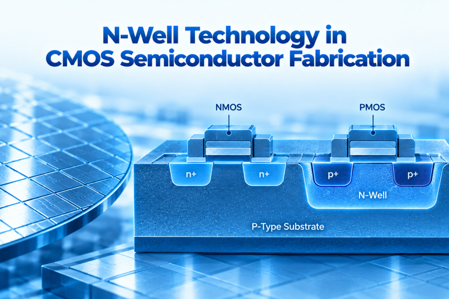
N-Well technology is a CMOS fabrication technique in which an n-type well is formed inside a p-type silicon substrate.
The N-well provides the body or bulk region in which PMOS transistors are fabricated, while NMOS transistors are typically formed directly in the surrounding p-type substrate.
A simplified structure can be represented as:
P-Type Substrate → N-Well Formation → PMOS Formation + NMOS Formation → CMOS Interconnection
The two transistor types require different body regions:
- NMOS: Formed in the p-type substrate
- PMOS: Formed inside the n-type well
This complementary arrangement allows CMOS circuits to use both NMOS and PMOS devices while achieving the low static power characteristics for which CMOS is widely known.
N-well technology became an important early approach for CMOS manufacturing because it provides a relatively straightforward method for integrating complementary MOS devices on the same substrate.
Why N-Well Is Important in CMOS Fabrication
The fundamental challenge in CMOS fabrication is creating complementary transistor structures with appropriate source, drain, body, and well connections.
For an NMOS transistor, the body region is p-type, while a PMOS transistor requires an n-type body region. N-well technology provides this additional n-type region within the p-type substrate.
Complementary Transistor Formation
The N-well makes it possible to fabricate PMOS devices alongside NMOS devices on the same silicon substrate.
Electrical Isolation
The well structure helps establish appropriate electrical regions for the different transistor types and supports proper body biasing.
Body Connection
The N-well is generally connected to an appropriate positive supply or well-bias potential so that the PMOS body remains correctly biased.
CMOS Logic Implementation
With NMOS and PMOS devices available together, designers can construct fundamental CMOS gates such as:
- Inverters
- NAND gates
- NOR gates
- Flip-flops
- Multiplexers
- Memory cells
- Complex logic circuits
Therefore, N-well formation is an important part of the underlying CMOS process flow.
N-Well CMOS Structure and Device Operation
A basic N-well CMOS structure contains an NMOS transistor in the p-type substrate and a PMOS transistor inside the N-well.
Consider a CMOS inverter.
The PMOS device is connected toward the positive supply, while the NMOS device is connected toward ground. Their gates are electrically connected as the input, and their drains are connected to form the output.
When Input Is LOW
The PMOS transistor turns ON while the NMOS transistor turns OFF.
The output is therefore pulled toward the positive supply, producing a logic HIGH.
When Input Is HIGH
The NMOS transistor turns ON while the PMOS transistor turns OFF.
The output is pulled toward ground, producing a logic LOW.
This complementary switching behavior is central to CMOS logic.
The N-well must also be maintained at the appropriate electrical potential. Proper well and substrate contacts are important for controlling body potential and reducing unwanted parasitic effects.
Applications and Evolution of N-Well CMOS Technology
N-well technology has played an important role in the development of CMOS integrated circuits and remains an essential concept for understanding semiconductor device fabrication.
Its principles are relevant to many types of integrated circuits, including:
- Digital logic circuits
- Microprocessors
- Microcontrollers
- Memory circuits
- Analog ICs
- Mixed-signal ICs
- System-on-Chip (SoC) devices
- Sensor interfaces
As CMOS technology has evolved, semiconductor manufacturers have introduced more advanced well and substrate architectures, including twin-well and triple-well structures, along with increasingly sophisticated isolation and body-bias techniques.
These approaches provide greater control over device isolation, substrate noise, latch-up behavior, and transistor characteristics.
The fundamental concept, however, remains important: different transistor types require carefully engineered semiconductor body regions to operate correctly within a CMOS architecture.
Conclusion
N-Well Technology is a fundamental concept in CMOS semiconductor fabrication, providing the n-type body region required for PMOS transistor formation within a p-type silicon substrate.
Through controlled well formation, doping, annealing, transistor fabrication, isolation, and interconnection, N-well CMOS technology enables NMOS and PMOS devices to operate together in complementary circuits.
Although modern semiconductor processes have evolved significantly beyond basic N-well structures, understanding this technology is essential for anyone studying CMOS fabrication, semiconductor process technology, VLSI design, device physics, and integrated circuit manufacturing.
As semiconductor devices continue to scale toward advanced process technologies, well engineering and substrate control remain important for achieving reliable transistor operation and high-performance integrated circuits.