
June 5, 2026 · Avecas Technologies
Fan-Out Wafer-Level Packaging (FOWLP): Powering Next-Generation Chips
As semiconductor devices continue to evolve, the demand for higher performance, lower power consumption, and smaller form factors is growing rapidly. While transistor scaling remains important, advanced packaging technologies have become equally critical in driving innovation. One such technology is Fan-Out Wafer-Level Packaging (FOWLP), which is enabling the next generation of high-performance and compact electronic devices.
What Is Fan-Out Wafer-Level Packaging (FOWLP)?
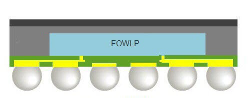
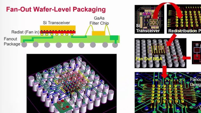
Fan-Out Wafer-Level Packaging (FOWLP) is an advanced semiconductor packaging technology that extends electrical connections beyond the boundaries of the chip using Redistribution Layers (RDLs). Unlike traditional packaging methods, FOWLP eliminates the need for a conventional substrate, resulting in a thinner, smaller, and more efficient package.
This innovative approach allows semiconductor manufacturers to increase connectivity while maintaining a compact footprint.
Why Is FOWLP Important?
Modern applications such as Artificial Intelligence (AI), 5G communications, automotive electronics, and high-performance computing require chips that deliver exceptional performance within limited space and power budgets.
FOWLP addresses these challenges by:
- Supporting higher I/O density
- Reducing package size and thickness
- Improving electrical performance
- Enhancing thermal management
- Lowering power consumption
- Enabling greater system integration
These advantages make FOWLP one of the most promising advanced packaging solutions available today.
How Does FOWLP Work?
The FOWLP manufacturing process involves several key steps:
Die Placement
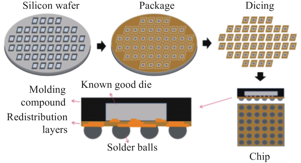
Individual semiconductor dies are placed onto a carrier wafer.
Molding and Encapsulation
A molding compound surrounds the dies, creating a reconstituted wafer structure.
Redistribution Layer (RDL) Formation
Metal interconnect layers are built over the reconstituted wafer to route signals beyond the chip boundaries.
Solder Ball Attachment
Solder balls are added to create external electrical connections.
Testing and Singulation
The packaged devices are tested and separated into individual units for final use.
This process enables highly integrated packages with improved performance characteristics.
Key Benefits of FOWLP
Improved Electrical Performance
Shorter interconnect paths reduce signal loss, resistance, and parasitic effects.
Compact Package Size
The absence of a traditional substrate allows thinner and smaller package designs.
Better Thermal Efficiency
Enhanced heat dissipation helps maintain performance and reliability.
Increased Design Flexibility
Engineers can integrate multiple functions within a single package.
Cost-Effective Manufacturing
Wafer-level processing can improve production efficiency and reduce packaging complexity.
Applications of FOWLP
FOWLP has become a preferred packaging technology across several industries:
Mobile Devices
Used in smartphone processors and advanced mobile applications requiring high performance in compact spaces.
Artificial Intelligence (AI)
Supports AI accelerators that demand high bandwidth and low latency.
5G Communication Systems
Enables high-speed RF and communication modules.
Automotive Electronics
Provides reliable and compact solutions for advanced driver assistance systems (ADAS) and autonomous vehicles.
High-Performance Computing
Helps deliver improved computing power while maintaining energy efficiency.
As electronic systems become more complex, FOWLP continues to expand into new application areas.
The Future of FOWLP
The semiconductor industry is increasingly focusing on advanced packaging to complement transistor scaling. Technologies such as chiplets, heterogeneous integration, and System-in-Package (SiP) architectures are driving the adoption of FOWLP.
Future developments are expected to bring:
- Higher interconnect density
- Improved package reliability
- Greater integration of multiple dies
- Enhanced support for AI and high-performance computing applications
- More advanced heterogeneous system designs
As a result, FOWLP is poised to play a central role in the future of semiconductor innovation.
Conclusion
Fan-Out Wafer-Level Packaging (FOWLP) is transforming the way semiconductor devices are packaged and integrated. By offering higher performance, improved thermal efficiency, greater design flexibility, and compact form factors, FOWLP is helping meet the demands of next-generation electronics. As advanced applications continue to grow, this packaging technology will remain a key enabler of future semiconductor breakthroughs.
Looking to build hands-on VLSI skills? CourseTron offers industry-aligned courses in VLSI design, verification, and semiconductor engineering.