
June 8, 2026 · Avecas Technologies
Backside Power Delivery: A Game-Changer for Future Chips
As semiconductor technology advances toward 2nm and beyond, traditional chip design approaches are reaching their physical limits. Engineers are facing growing challenges related to power delivery, routing congestion, performance, and energy efficiency. One of the most promising innovations addressing these issues is Backside Power Delivery (BSPD).
By moving power distribution networks from the front side of the chip to the backside of the silicon wafer, BSPD opens new possibilities for higher performance, lower power consumption, and improved transistor density. Major semiconductor manufacturers are investing heavily in this technology as a key enabler for next-generation processors.
The Problem with Traditional Power Delivery
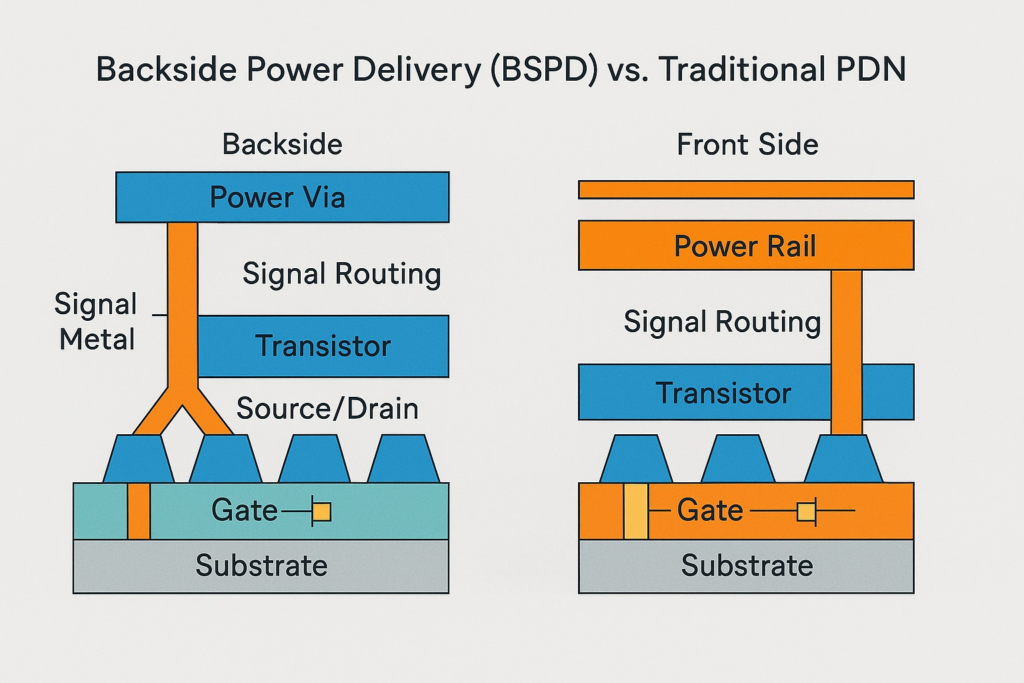
In conventional chip designs, both signal interconnects and power delivery networks share the same metal layers on the front side of the wafer.
This approach has worked well for decades, but as transistor density continues to increase, several problems emerge:
- Routing congestion becomes severe.
- Power and signal lines compete for valuable metal resources.
- Increased resistance causes larger voltage drops (IR Drop).
- Higher current densities increase electromigration risks.
- Performance scaling becomes more difficult at advanced nodes.
As billions of transistors are packed into increasingly smaller areas, traditional power delivery methods are becoming a significant bottleneck.
What Is Backside Power Delivery?
Backside Power Delivery is a new chip architecture that separates power routing from signal routing.
Instead of delivering power through the front-side metal layers, dedicated power connections are created from the backside of the silicon wafer directly to the transistor layer.
In this architecture:
- Front side metal layers primarily handle signal routing.
- Backside metal layers handle power distribution.
- Power reaches transistors through specialized vertical connections.
- Signal and power networks are physically separated.
This separation dramatically improves routing efficiency and power delivery performance.
Key Benefits of Backside Power Delivery
Improved Performance
With less routing congestion on the front side, signal paths become shorter and more efficient.
Benefits include:
- Faster signal propagation.
- Higher operating frequencies.
- Improved overall chip performance.
Reduced Power Loss
Power can reach transistors through shorter and lower-resistance paths.
Advantages include:
- Lower IR Drop.
- Better voltage stability.
- Improved energy efficiency.
Increased Transistor Density
Since power lines no longer occupy valuable front-side routing resources, additional space becomes available for signal routing and logic implementation.
This allows:
- Higher transistor density.
- Better area utilization.
- More functionality within the same die size.
Enhanced Reliability
Backside power networks reduce current density in front-side interconnects.
This helps minimize:
- Electromigration.
- Thermal hotspots.
- Long-term reliability issues.
Challenges and Future Outlook
Despite its advantages, BSPD introduces new manufacturing complexities.
Key challenges include:
- Wafer thinning processes.
- Backside alignment accuracy.
- Additional fabrication costs.
- Thermal management considerations.
- Advanced packaging integration requirements.
However, the benefits significantly outweigh the challenges.
As the semiconductor industry moves toward Angstrom-era technologies, Backside Power Delivery is expected to become a standard feature in advanced nodes.
Combined with innovations such as:
- Gate-All-Around transistors,
- CFET architectures,
- Chiplet-based designs,
- 3D integration,
BSPD will play a critical role in sustaining performance scaling beyond traditional Moore’s Law limits.
Conclusion
Backside Power Delivery represents one of the most important architectural innovations in modern semiconductor manufacturing. By separating power delivery from signal routing, it addresses some of the industry’s biggest challenges, including routing congestion, IR drop, power efficiency, and transistor density limitations.
As advanced process nodes continue to evolve, technologies like Intel PowerVia and TSMC’s Super Power Rail are paving the way for faster, more efficient, and more reliable chips. For AI processors, data center hardware, and future high-performance computing systems, Backside Power Delivery is not just an improvement—it is a fundamental shift in how chips are designed and powered.
The future of semiconductor scaling may very well depend on what happens on the backside of the wafer.
Looking to build hands-on VLSI skills? CourseTron offers industry-aligned courses in VLSI design, verification, and semiconductor engineering.