
June 16, 2026 · Avecas Technologies
System-in-Package (SiP): The Next Step in Integration
The semiconductor industry is continuously pushing the boundaries of performance, size, and efficiency. As traditional transistor scaling becomes more challenging, advanced packaging technologies are becoming the key drivers of innovation.
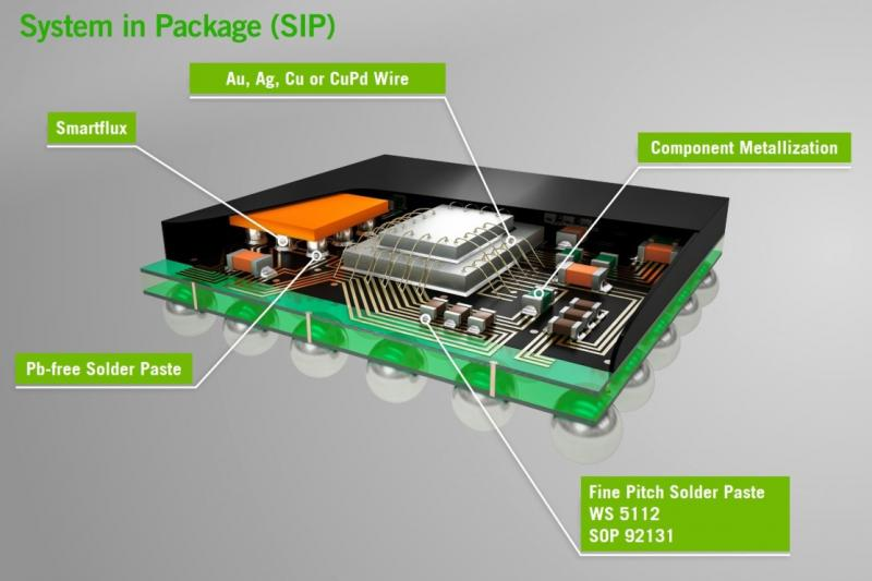
System-in-Package (SiP) represents the next generation of integration by combining multiple semiconductor components into a single package. Instead of placing all functions on one large chip, SiP integrates processors, memory, sensors, RF modules, power management ICs, and other components into a compact system.
This approach enables higher performance, smaller form factors, and faster product development for modern electronic applications.
What is System-in-Package (SiP)?
System-in-Package (SiP) is an advanced semiconductor packaging technology where multiple dies or functional components are assembled together inside one package to operate as a complete system.
A SiP module can include:
- Application processors
- Memory chips
- Analog and digital circuits
- Communication modules
- Sensors and controllers
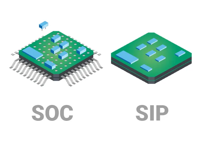
Unlike traditional System-on-Chip (SoC), where all functions are fabricated on a single silicon die, SiP combines different chips using advanced packaging techniques.
This allows designers to select the best technology for each component while improving overall system performance.
Why SiP is Transforming the Semiconductor Industry
Modern applications demand high computing power with lower power consumption and smaller device sizes. SiP addresses these challenges by providing:
Higher Integration Density
Multiple chips are placed closer together, reducing system size and improving efficiency.
Better Performance
Shorter connections between components enable faster data transfer and reduced latency.
Cost Optimization
Different components can be manufactured using optimized processes, reducing development costs.
Faster Innovation
Designers can integrate existing chiplets and modules instead of creating a complete chip from scratch.
SiP is becoming a major technology for advanced electronics where space and performance are critical.
SiP vs SoC: The New Integration Approach
Traditional SoC technology integrates all functions into a single silicon die. While powerful, it faces challenges such as higher design complexity, increased manufacturing costs, and scaling limitations.
SiP provides a flexible alternative by combining multiple specialized chips in one package.
Key differences:
- SoC: One large chip with multiple functions
- SiP: Multiple optimized chips combined into one system
With the rise of chiplet-based designs, SiP is creating a new path beyond conventional scaling.
Applications Driving SiP Growth
SiP technology is already powering several advanced industries:
Smartphones & Wearables
Compact modules combine processors, memory, sensors, and communication circuits.
Automotive Electronics
Used in ADAS, autonomous driving systems, and intelligent vehicle platforms.
IoT Devices
Enables small, low-power connected devices.
Artificial Intelligence & Data Centers
Supports high-performance computing through advanced multi-chip integration.
Medical Electronics
Helps create smaller and smarter diagnostic devices.
Future of SiP: The Era of Advanced Packaging
As semiconductor scaling slows down, advanced packaging technologies like SiP, 2.5D integration, 3D stacking, and chiplets are becoming essential for future computing.
The future will focus on combining specialized chips rather than building a single massive processor. SiP will continue to improve through:
- Higher-density interconnects
- 3D chip stacking
- Advanced thermal management
- Faster chip-to-chip communication
System-in-Package is not just a packaging method it is becoming a foundation for the next generation of semiconductor innovation.
Looking to build hands-on VLSI skills? CourseTron offers industry-aligned courses in VLSI design, verification, and semiconductor engineering.