

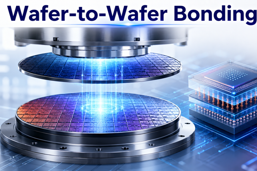
As semiconductor technology continues to scale, simply shrinking transistor dimensions is no longer enough to deliver the performance and integration required by modern applications. Advanced computing, artificial intelligence, high-bandwidth memory, and heterogeneous systems increasingly require multiple semiconductor layers to be integrated vertically.
Wafer-to-Wafer (W2W) Bonding is an advanced semiconductor packaging and integration technology that enables two complete semiconductor wafers to be permanently joined together. Instead of connecting individual dies one at a time, entire wafers are aligned and bonded, creating a highly dense vertical connection between semiconductor layers.
What is Wafer-to-Wafer Bonding?
Wafer-to-Wafer Bonding is a process in which two semiconductor wafers are precisely aligned and joined to form a single integrated structure. The bonding interface can provide either mechanical attachment, electrical connectivity, or both, depending on the bonding technology used.
The basic process involves:
- Preparing and cleaning both wafer surfaces.
- Creating the required bonding structures.
- Aligning the wafers with nanometer-level precision.
- Bringing the surfaces into contact.
- Applying appropriate thermal, pressure, or plasma-based treatments.
- Strengthening the bond through a controlled process.
- Performing subsequent thinning and fabrication steps when required.
Several bonding approaches are used in advanced semiconductor manufacturing, including direct bonding, oxide bonding, metal bonding, and hybrid bonding.
Why is Wafer-to-Wafer Bonding Important?
Traditional packaging approaches often rely on horizontal connections between semiconductor dies. As the demand for higher bandwidth and greater integration increases, these connections can become a significant performance bottleneck.
Wafer-to-Wafer Bonding provides several important advantages:
- Enables high-density 3D integration
- Reduces interconnect distance
- Improves signal bandwidth
- Reduces communication latency
- Supports compact device architectures
- Enables heterogeneous integration
- Provides high interconnect density
- Can reduce system-level power consumption
- Supports advanced memory architectures
- Enables integration of different semiconductor layers
Applications
Wafer-to-Wafer Bonding is used in a growing range of semiconductor applications, including:
- 3D Integrated Circuits
- Advanced memory devices
- CMOS image sensors
- High-Bandwidth Memory (HBM)
- Logic-on-memory integration
- 3D NAND architectures
- Image and sensing technologies
- Heterogeneous semiconductor integration
- Advanced chiplet architectures
- High-performance computing systems
Conclusion
Wafer-to-Wafer Bonding is emerging as a key technology for overcoming the limitations of conventional planar semiconductor integration. By joining complete wafers with extremely precise alignment, it enables dense vertical architectures, shorter interconnects, higher bandwidth, and improved system-level integration.
As the industry advances toward 3D ICs, hybrid bonding, chiplets, heterogeneous integration, and advanced memory architectures, wafer bonding will become increasingly important in semiconductor manufacturing and packaging.