

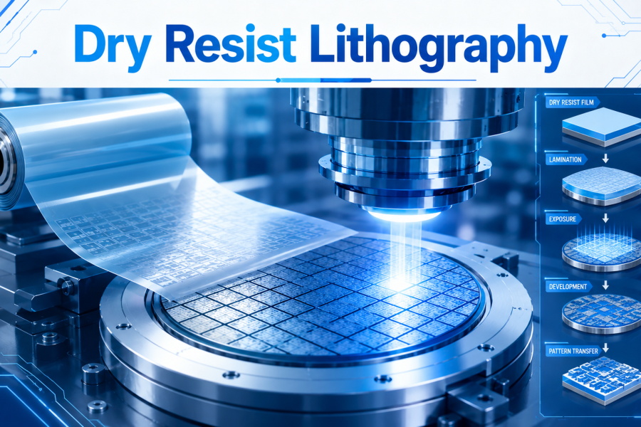
As semiconductor devices continue to become smaller and more complex, lithography processes must deliver increasingly precise patterns while maintaining productivity, consistency, and process stability. Dry resist lithography is emerging as an important approach for addressing these demands.
Unlike conventional liquid photoresists, dry resist materials are applied as a solid film, offering improved control over resist thickness, reduced solvent use, and opportunities for more uniform wafer processing. This technology is gaining attention for advanced semiconductor manufacturing, particularly where fine features and reliable pattern transfer are critical.
What Is Dry Resist Lithography?
Dry resist lithography is a semiconductor patterning technique that uses a pre-formed solid resist film rather than a liquid photoresist.
The dry resist film is laminated or otherwise transferred onto the wafer surface and then exposed using a lithography system. After exposure, the resist undergoes development to create the desired pattern, which can subsequently be transferred into the underlying material through etching or other processing steps.
The basic process can be summarized as:
Dry Resist Film → Lamination → Exposure → Development → Pattern Transfer
This approach provides an alternative to conventional spin-coated resist processes and can offer advantages in specific advanced manufacturing applications.
Why Dry Resist Is Important for Advanced Manufacturing
One of the major attractions of dry resist technology is its potential to improve process uniformity and material efficiency.
Because the resist is supplied as a controlled film, its thickness can be engineered before it reaches the wafer. This can help reduce some of the challenges associated with liquid resist coating, particularly for applications requiring relatively thick or highly uniform films.
Dry resist processing can also reduce the amount of liquid solvent-based material required during coating. This creates opportunities for more efficient material usage and potentially simpler process integration.
For advanced semiconductor manufacturing, these characteristics can become increasingly valuable as wafer processing requirements become more demanding.
Key Advantages and Challenges
Dry resist lithography offers several potential advantages:
- Excellent film-thickness control for demanding applications
- Reduced solvent consumption compared with conventional liquid coating
- Good uniformity across processed substrates when properly laminated
- Potentially lower material waste
- Compatibility with specialized advanced packaging and patterning applications
- Improved process flexibility for selected high-resolution structures
However, the technology also presents challenges. Film lamination must be carefully controlled to prevent bubbles, wrinkles, contamination, and other defects. Adhesion between the resist and wafer surface is also critical.
In addition, dry resist materials must provide the right balance between sensitivity, resolution, mechanical strength, and etch resistance. These requirements can make material development and process optimization particularly important.
Applications in Semiconductor and Advanced Packaging
Dry resist technology is attracting interest across several areas of semiconductor manufacturing and advanced packaging.
It can be particularly useful for thick-film patterning, redistribution layers, bump formation, interconnect structures, and other applications where conventional liquid resist processing may face limitations.
As advanced packaging increasingly incorporates chiplets, high-density interconnects, and heterogeneous integration, precise and reliable patterning becomes essential. Dry resist approaches can support these processes by providing engineered film thickness and robust patterning characteristics.
The technology may also play a role in future manufacturing environments where improved material efficiency and process control are increasingly important.
Conclusion
Dry resist lithography provides a compelling alternative to traditional liquid photoresist processing for selected semiconductor and advanced packaging applications. By using a pre-formed resist film, the technology offers opportunities for improved thickness control, material efficiency, and process uniformity.
While challenges such as adhesion, defect management, and high-resolution patterning remain, continued innovation could make dry resist lithography increasingly valuable as semiconductor manufacturing moves toward more advanced and complex structures.