

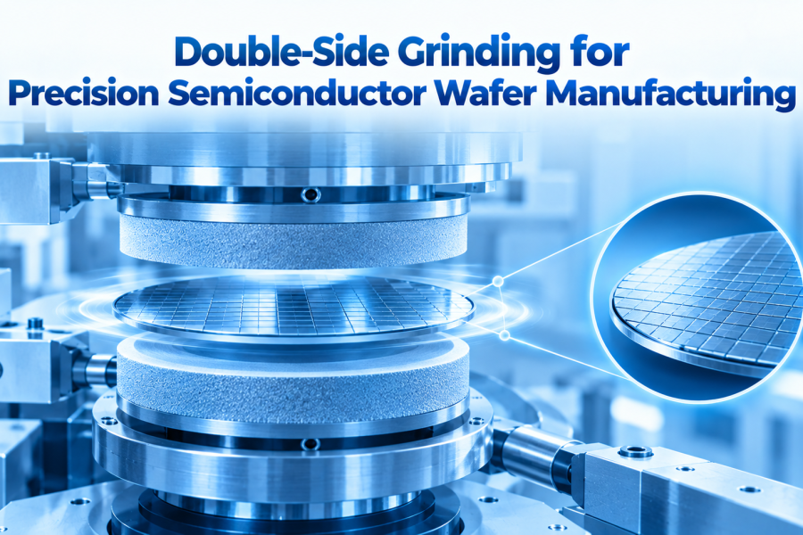
As semiconductor devices continue to become smaller, thinner, and more complex, wafer manufacturing requires increasingly precise control over thickness, flatness, surface quality, and dimensional uniformity. These characteristics directly influence downstream processes such as lithography, bonding, packaging, and wafer handling.
Double-Side Grinding (DSG) is an important wafer thinning and surface preparation technology designed to process both sides of a semiconductor wafer with high precision. By simultaneously grinding the front and back surfaces, DSG can achieve controlled wafer thickness and improved geometric uniformity while supporting high-volume semiconductor manufacturing.
What Is Double-Side Grinding?
Double-Side Grinding is a semiconductor wafer manufacturing process in which the front and back surfaces of a wafer are ground simultaneously using abrasive grinding wheels.
Unlike single-side grinding, where one surface is processed at a time, double-side grinding removes material from both surfaces in a controlled manner.
A simplified process can be represented as:
Wafer Loading → Alignment → Double-Side Grinding → Cleaning → Inspection → Final Surface Preparation
During grinding, the wafer is typically positioned between two grinding wheels. The controlled movement of the wheels removes material from both sides while maintaining the required wafer thickness and geometry.
Double-side grinding is particularly valuable when semiconductor wafers require tight control of:
- Total thickness
- Thickness variation
- Flatness
- Parallelism
- Surface roughness
- Edge geometry
The process can be used as part of the wafer preparation flow before subsequent polishing or other surface-finishing operations.
Why Double-Side Grinding Matters in Semiconductor Manufacturing
Wafer geometry plays an important role in semiconductor manufacturing. Variations in thickness or flatness can create problems during subsequent processing and may affect wafer handling and device yield.
Precise Thickness Control
Modern semiconductor applications often require wafers to meet tightly controlled thickness specifications. Double-side grinding provides an efficient method for removing material while controlling the final wafer thickness.
Improved Wafer Flatness
Processing both surfaces together can help achieve improved wafer geometry and reduce unwanted thickness variations.
High-Volume Processing
Because both sides are processed simultaneously, DSG can provide high material-removal efficiency and support high-throughput wafer manufacturing.
Preparation for Advanced Packaging
Thinner wafers are increasingly important for applications such as 3D integration, wafer bonding, stacked devices, and advanced semiconductor packaging.
Consistent Wafer Geometry
Uniform wafer geometry supports downstream processes that depend on accurate wafer positioning, handling, alignment, and surface contact.
For these reasons, double-side grinding is an important part of precision wafer manufacturing.
Key Advantages of Double-Side Grinding
Double-side grinding offers several advantages for precision semiconductor wafer manufacturing.
High Material Removal Rate
Processing both surfaces simultaneously can significantly improve material-removal efficiency compared with sequential single-side operations.
Better Thickness Uniformity
Controlled grinding from both sides can help maintain consistent wafer thickness across the processed area.
Improved Parallelism
The simultaneous processing of opposite surfaces can support better control of the relationship between the two wafer surfaces.
Reduced Processing Time
Because both surfaces are processed during the same operation, DSG can reduce the number of processing steps required for certain wafer preparation flows.
Suitable for Wafer Thinning
DSG is useful for applications requiring wafers to be reduced from their initial thickness to a controlled thinner profile.
Scalability
Automated double-side grinding systems can be integrated into high-volume manufacturing environments where repeatability and throughput are critical.
These advantages make DSG particularly relevant to precision wafer preparation and advanced semiconductor manufacturing.
Applications and Future of Double-Side Grinding
Double-side grinding is used across multiple areas of semiconductor wafer manufacturing and advanced device production.
Silicon Wafer Manufacturing
DSG can be used during the preparation and dimensional control of silicon wafers before subsequent surface-finishing operations.
Power Semiconductors
Power devices often require controlled wafer thickness and backside processing to support electrical and thermal performance requirements.
MEMS Manufacturing
Microelectromechanical systems can require precise substrate thickness and geometry, making controlled wafer grinding an important manufacturing capability.
Advanced Packaging
Thinned wafers are increasingly important for 3D ICs, wafer-level packaging, wafer bonding, stacked dies, and heterogeneous integration.
Compound Semiconductor Wafers
Materials such as silicon carbide and other compound semiconductor substrates can require specialized grinding and finishing approaches to achieve the required surface and geometric characteristics.
As semiconductor manufacturing moves toward thinner wafers, larger wafer formats, advanced bonding, and increasingly precise device architectures, grinding technology will continue to evolve.
Future developments are expected to focus on improved automation, real-time process monitoring, advanced abrasive technologies, reduced subsurface damage, and tighter integration between grinding, polishing, cleaning, and metrology.
Conclusion
Double-Side Grinding is a critical precision process for achieving the thickness, flatness, and geometric control required in modern semiconductor wafer manufacturing. By processing both wafer surfaces simultaneously, DSG can provide high material-removal efficiency while supporting tight dimensional specifications.
Although challenges such as surface damage, wafer stress, thickness variation, edge damage, and contamination must be carefully managed, advances in grinding equipment, abrasive technology, automation, inspection, and metrology continue to improve the process.
As semiconductor manufacturing advances toward thinner wafers, power devices, MEMS, 3D integration, wafer bonding, and advanced packaging, precision wafer grinding will remain an essential technology in the semiconductor manufacturing ecosystem.