

As artificial intelligence (AI), high-performance computing (HPC), advanced networking, and chiplet-based architectures continue to evolve, the semiconductor industry is facing increasing demands for higher bandwidth, greater transistor density, and improved power efficiency. While transistor innovation remains important, advancements in semiconductor packaging are becoming equally critical to overall system performance.
Glass Core Substrates are emerging as a next-generation packaging technology that replaces conventional organic substrates with engineered glass materials. Offering superior dimensional stability, excellent electrical performance, and the ability to support ultra-high-density interconnections, glass core substrates are expected to play a pivotal role in future semiconductor packaging for AI processors, advanced memory, and heterogeneous integration.
What are Glass Core Substrates?
A Glass Core Substrate is an advanced semiconductor packaging platform that uses ultra-flat, high-strength glass as the core material for integrated circuit packaging instead of traditional organic laminate substrates.
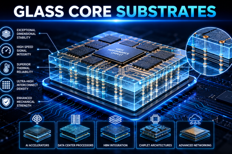
The glass core acts as a stable mechanical and electrical foundation that supports multiple semiconductor dies, chiplets, memory devices, and high-speed interconnects. Through precision fabrication techniques, the substrate incorporates Through-Glass Vias (TGVs), redistribution layers (RDLs), and fine-pitch wiring to enable high-density chip integration.
Compared with conventional packaging materials, glass offers improved dimensional accuracy, reduced warpage, and better signal integrity, making it ideal for future high-performance semiconductor systems.
Why are Glass Core Substrates Important?
As semiconductor packages become larger and more complex, traditional organic substrates face limitations in maintaining dimensional stability and supporting extremely fine interconnect pitches.
Glass Core Substrates address these challenges by providing several significant advantages:
- Exceptional dimensional stability
- Ultra-low package warpage
- Higher interconnect density
- Improved signal integrity for high-speed interfaces
- Lower electrical loss at high frequencies
- Better thermal and mechanical reliability
- Support for larger package sizes
- Enhanced scalability for chiplet architectures
Applications
Glass Core Substrates are expected to become a key enabling technology across several advanced semiconductor applications, including:
- Artificial Intelligence (AI) accelerators
- High-Performance Computing (HPC) processors
- High-Bandwidth Memory (HBM) integration
- Chiplet-based processor architectures
- Data center processors
- Cloud computing infrastructure
- Advanced networking and optical communication systems
- 2.5D and 3D heterogeneous integration
- Next-generation server platforms
Conclusion
Glass Core Substrates represent a significant advancement in semiconductor packaging by offering a stronger, more stable, and electrically superior alternative to conventional organic substrates. Their ability to support ultra-high-density interconnects, minimize signal loss, and enable large-scale chiplet integration positions them as a cornerstone technology for the next era of semiconductor innovation.
With the rapid growth of AI, high-performance computing, advanced memory, and heterogeneous integration, Glass Core Substrates are set to become a foundational technology in future semiconductor manufacturing. As research and commercial adoption continue to accelerate, they will play a vital role in enabling faster, more efficient, and highly integrated semiconductor systems.