

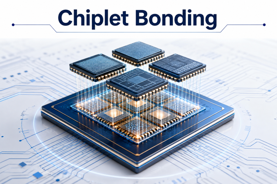
As semiconductor systems become more complex, traditional monolithic chip design is increasingly challenged by manufacturing costs, yield limitations, power consumption, and the difficulty of integrating different technologies on a single die. Chiplet technology offers a flexible alternative by dividing a large system into smaller functional dies called chiplets and integrating them within a single package.
Chiplet bonding is the critical packaging process that physically and electrically connects these individual chiplets. Instead of manufacturing one large die, designers can combine chiplets optimized for different functions, process nodes, or technologies. This approach enables high-performance processors, AI accelerators, networking devices, memory systems, and other advanced semiconductor products to be built using a modular architecture.
What Is Chiplet Bonding?
Chiplet bonding refers to the techniques used to attach and interconnect multiple semiconductor dies inside an advanced package. The bonding process must establish reliable mechanical, electrical, and thermal connections between chiplets while maintaining extremely precise alignment.
Depending on the application, chiplets can communicate through different interconnect structures, including:
- Microbumps for fine-pitch die-to-die connections
- Copper-to-copper hybrid bonding for very high-density interconnects
- Silicon interposers that provide routing between chiplets
- Organic substrates for package-level connectivity
- Direct die-to-die bonding for advanced three-dimensional integration
The objective is to create short, high-bandwidth communication paths while minimizing signal loss, latency, power consumption, and package size.
Key Chiplet Bonding Technologies
Several bonding approaches are being developed and adopted for chiplet-based architectures.
Microbump Bonding
Microbumps are small solder-based connections positioned between two dies. They provide both mechanical attachment and electrical connectivity. This technique is widely used in advanced packaging because it supports relatively high interconnect density while remaining compatible with established semiconductor packaging processes.
Hybrid Bonding
Hybrid bonding combines dielectric bonding with direct metal-to-metal connections, commonly using copper. Because it eliminates or significantly reduces the need for conventional solder bumps, hybrid bonding can achieve extremely fine interconnect pitches.
This makes it particularly attractive for high-density chiplet integration and 3D semiconductor architectures where very short electrical paths are required.
Interposer-Based Integration
In 2.5D packaging, chiplets are mounted on an interposer that provides high-density routing between the dies. Silicon interposers can support thousands of interconnections and are especially useful for integrating high-performance computing dies with high-bandwidth memory.
Why Chiplet Bonding Matters
Chiplet bonding is becoming increasingly important because it addresses several limitations of conventional semiconductor scaling.
Improved manufacturing flexibility: Different chiplets can be manufactured using the process technology best suited to their functions. A high-performance compute chiplet, for example, may use an advanced process node while an I/O chiplet can use a more mature and cost-effective technology.
Higher manufacturing yield: Smaller dies generally have a lower probability of containing a manufacturing defect. Building a system from multiple smaller chiplets can therefore improve overall manufacturing economics.
Design flexibility: Chiplets allow semiconductor designers to create modular systems by combining computing, memory, I/O, networking, and accelerator functions.
Performance improvements: Short die-to-die connections can provide high bandwidth and lower latency compared with traditional board-level communication.
Cost optimization: Not every function in a system requires the most advanced process node. Chiplet architectures can reduce costs by using advanced technologies only where they provide meaningful benefits.
The Future of Chiplet Bonding
The future of chiplet bonding is closely connected to the development of advanced 2.5D and 3D semiconductor packaging. As conventional transistor scaling becomes more challenging and expensive, system-level innovation through advanced packaging is becoming increasingly important.
Future bonding technologies are expected to support finer interconnect pitches, higher bandwidth, improved power efficiency, greater 3D integration, and better thermal performance. Hybrid bonding is particularly promising because its high interconnect density can enable chiplets to communicate almost like components on a single large die.
Chiplet architectures are also expected to play an important role in AI computing, high-performance computing, data centers, automotive electronics, networking, and heterogeneous integration.
Conclusion
Chiplet bonding is transforming semiconductor packaging from a supporting manufacturing step into a major driver of system-level performance. By enabling multiple specialized dies to work together inside a single package, chiplet technology provides a practical path toward building larger, faster, and more flexible semiconductor systems.
As bonding technologies continue to improve, the combination of chiplets, advanced interconnects, 2.5D packaging, and 3D integration is likely to become a central strategy for the next generation of semiconductor innovation.