

As semiconductor technology advances toward 2 nm, 1.4 nm, and beyond, conventional etching techniques face increasing challenges in controlling extremely small features. Modern transistors and interconnect structures require precise material removal without damaging the surrounding layers.
Digital Etching is an advanced semiconductor fabrication approach designed to provide highly controlled, repeatable material removal at the nanoscale. Unlike conventional continuous etching, digital etching uses precisely controlled, self-limiting process cycles to remove material in extremely small increments.
This technology is particularly valuable for advanced transistor fabrication, three-dimensional structures, and applications where conventional plasma etching may lack the required precision.
What is Digital Etching?
Digital Etching is a cyclic etching technique in which material is removed through a sequence of carefully controlled surface-modification and removal steps.
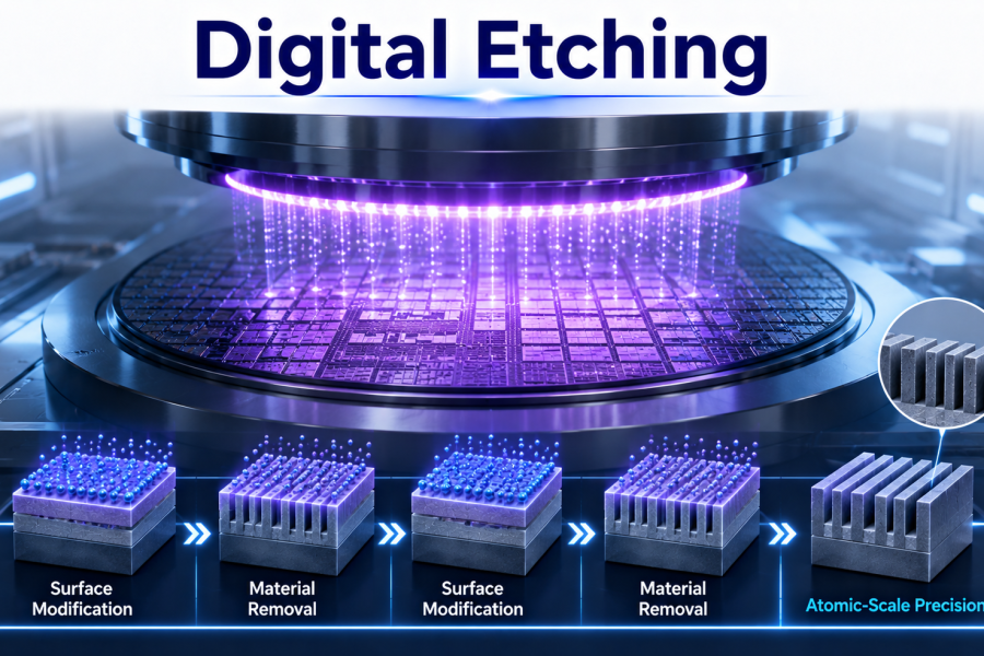
Instead of continuously etching a material, the process performs repeated cycles. Each cycle modifies or activates a very thin surface layer, followed by a selective removal step. Because the process can be designed to be highly controlled or self-limiting, the amount of material removed per cycle can be precisely regulated.
A simplified digital etching sequence can be represented as:
Surface Modification → Material Removal → Surface Modification → Material Removal → Repeat
By controlling the number of cycles, semiconductor manufacturers can achieve extremely accurate etch depths and dimensions.
Digital Etching is closely related to advanced techniques such as Atomic Layer Etching (ALE), although the exact chemistry and process implementation can vary depending on the material and application.
Why is Digital Etching Important?
As semiconductor dimensions shrink, even a small amount of uncontrolled material removal can significantly affect transistor performance and manufacturing yield. Digital Etching provides greater control over the etching process and helps address several scaling challenges.
Applications
Digital Etching has significant potential across advanced semiconductor manufacturing and emerging device architectures.
Key applications include:
- Gate-All-Around (GAA) transistors
- FinFET structures
- Nanosheet and nanowire devices
- 3D semiconductor structures
- Advanced memory devices
- High-density logic circuits
- Selective material removal
- Semiconductor surface engineering
- Advanced power devices
- Next-generation process nodes
Conclusion
Digital Etching represents an important evolution in semiconductor process technology by providing controlled, cyclic material removal at extremely small scales. Instead of relying solely on continuous etching, it enables manufacturers to carefully engineer the surface and remove material in precisely controlled increments.
As semiconductor devices become smaller and increasingly three-dimensional, controlling etch depth, selectivity, surface damage, and critical dimensions becomes essential. Digital Etching provides a pathway toward this level of process precision.
With continued development in plasma chemistry, surface engineering, and process control, Digital Etching will play an increasingly important role in advanced transistor fabrication, 3D semiconductor structures, and future technology nodes, helping manufacturers push semiconductor scaling beyond today’s limits.