

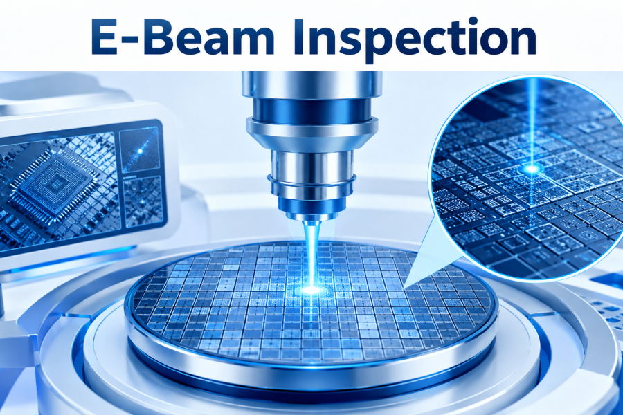
As semiconductor devices continue to shrink toward advanced process nodes, detecting defects that are only a few nanometers in size has become increasingly challenging. Traditional optical inspection remains valuable for high-speed wafer monitoring, but its resolution can become a limiting factor when defects approach or fall below the optical wavelength scale.
This is where E-Beam Inspection (EBI) becomes critical.
E-Beam Inspection uses a focused beam of electrons to scan semiconductor wafers and examine extremely small structures with high-resolution imaging. It provides semiconductor manufacturers with a powerful way to identify defects, process variations, and pattern abnormalities that may be difficult to resolve using optical techniques.
What Is E-Beam Inspection?
E-Beam Inspection is a semiconductor inspection technique that uses a finely focused electron beam to scan across the surface of a wafer.
When the electron beam interacts with the wafer, it generates signals such as secondary electrons and backscattered electrons. These signals are collected and converted into high-resolution images or inspection data.
Unlike optical inspection, which relies on photons, EBI uses electrons with very short effective wavelengths. This enables significantly higher spatial resolution and makes it possible to examine nanoscale structures.
Why Is E-Beam Inspection Important for Advanced Nodes?
As semiconductor geometries shrink, manufacturing tolerances become increasingly tight.
A defect that might have been insignificant at a larger process node can become electrically or functionally critical at an advanced node.
E-Beam Inspection helps manufacturers investigate issues including:
- Nanometer-scale pattern defects
- Line-edge and line-width variations
- Missing or extra features
- Bridges and opens
- Pattern collapse
- Lithography-related defects
- Etch and deposition abnormalities
- EUV-related pattern imperfections
- Contact and via defects
- Random process defects
One of its major strengths is high-resolution defect characterization.
Optical inspection can rapidly examine large wafer areas, while EBI can provide much more detailed information about suspicious regions.
This makes the two technologies complementary rather than simply competing inspection methods.
The Future of E-Beam Inspection
The semiconductor industry is moving toward increasingly complex structures, smaller dimensions, and new materials. As this happens, the need for high-resolution inspection continues to grow.
Future E-Beam Inspection systems are expected to focus on improving:
- Inspection throughput
- Defect detection sensitivity
- Automated defect classification
- AI-assisted image analysis
- Design-aware inspection
- Multi-beam electron inspection
- Data processing efficiency
- Process control integration
One particularly important direction is multi-beam inspection, where multiple electron beams can inspect different areas simultaneously. This approach aims to retain the resolution advantages of electron-beam inspection while significantly improving throughput.
As semiconductor manufacturing approaches increasingly demanding geometries, E-Beam Inspection will play an important role in understanding whether fabricated structures match the intended design and in identifying process problems before they propagate through high-value wafer production.
Conclusion
E-Beam Inspection provides semiconductor manufacturers with a powerful high-resolution window into nanoscale manufacturing.
Its ability to visualize and characterize extremely small defects makes it especially valuable for advanced semiconductor processes. Although throughput and data-processing challenges remain, continued development in multi-beam technology, automation, and AI-based analysis could make EBI increasingly powerful in future fabs.
In semiconductor manufacturing, seeing smaller defects earlier can mean solving process problems before they become costly yield problems and E-Beam Inspection is one of the technologies making that possible.