

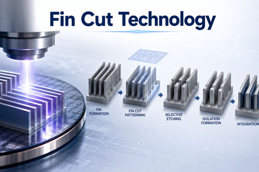
As semiconductor devices continue to shrink, manufacturers need increasingly precise techniques to define and shape microscopic features on silicon wafers. Fin Cut Technology is an important patterning approach used in advanced FinFET manufacturing to modify and isolate fin structures with high dimensional accuracy.
By enabling selective cutting of semiconductor fins, the technology helps manufacturers create the required transistor layouts while supporting tighter design rules and advanced process nodes.
What Is Fin Cut Technology?
In a FinFET, narrow vertical silicon structures called fins form an essential part of the transistor architecture. These fins are patterned across the wafer and later need to be selectively separated or modified according to the circuit layout.
Fin Cut Technology introduces a dedicated patterning and etching process to remove selected portions of these fins. This creates electrical isolation between specific transistor regions and allows the original continuous fin pattern to be converted into the required device structure.
The process therefore plays a key role in translating circuit-level designs into precisely defined physical transistor structures.
Why Is Fin Cut Technology Important?
Fin cut processes provide greater flexibility in advanced transistor layout and help semiconductor manufacturers achieve increasingly dense designs.
Key benefits include:
Improved transistor isolation: Selective fin removal helps electrically separate device regions.
Higher layout flexibility: Fin structures can be divided according to the requirements of different circuit designs.
Advanced-node compatibility: Fin cut techniques support the increasingly demanding patterning requirements of scaled FinFET technologies.
Better process control: Precise lithography and etching enable manufacturers to define extremely small features with controlled dimensions.
Together, these capabilities contribute to reliable transistor formation and improved utilization of wafer area.
Challenges in Advanced Fin Cut Processes
As semiconductor dimensions shrink, Fin Cut Technology becomes more challenging to implement. Pattern placement must remain highly accurate, while etching needs to provide sufficient selectivity without damaging surrounding structures.
Major challenges include:
- Overlay accuracy between the fin pattern and cut pattern
- Critical-dimension control at extremely small geometries
- Etch selectivity and profile control
- Pattern variability across the wafer
- Defect control during lithography and etching
- Process integration with other advanced transistor fabrication steps
These challenges require sophisticated lithography, metrology, etching, and process-control technologies.
The Future of Fin Patterning
Fin Cut Technology represents an important stage in the evolution of semiconductor patterning. As transistor architectures continue to evolve beyond conventional FinFET structures toward technologies such as gate-all-around architectures, patterning strategies are also becoming more sophisticated.
The continued development of advanced lithography, selective etching, process control, and computational techniques will remain essential for producing smaller and more complex semiconductor structures.
Conclusion
Fin Cut Technology demonstrates how seemingly small patterning steps can have a major impact on semiconductor device manufacturing. By precisely modifying fin structures, manufacturers can achieve the isolation, layout flexibility, and dimensional control required for advanced transistor technologies.
As semiconductor scaling continues, technologies that provide greater precision, tighter process control, and reliable pattern transfer will remain fundamental to the development of next-generation chips.