

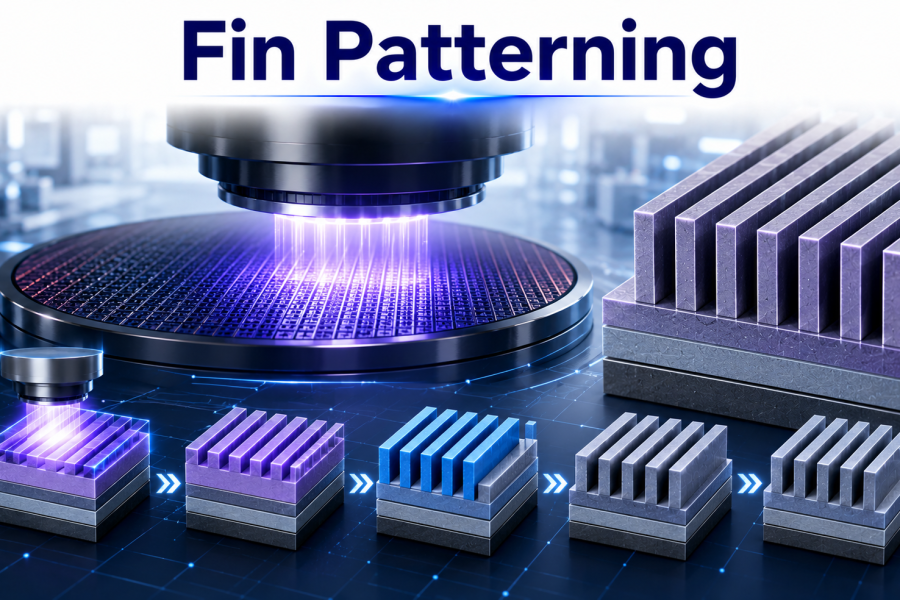
As semiconductor devices continue to scale, conventional planar transistors face increasing challenges in controlling leakage current, maintaining performance, and achieving higher transistor density. The industry responded with three-dimensional transistor architectures such as the FinFET, where the transistor channel is formed in a narrow vertical silicon structure called a fin.
At the heart of FinFET manufacturing is Fin Patterning the lithography and etching process used to create these precisely defined nanoscale fins. The dimensions, spacing, height, and uniformity of the fins directly influence transistor performance, power consumption, and manufacturing yield.
As semiconductor manufacturing progresses toward advanced nodes, increasingly sophisticated patterning techniques are required to create smaller and more uniform fins.
What is Fin Patterning?
Fin Patterning is the semiconductor fabrication process used to define and form the narrow, elongated silicon structures that serve as the channels of FinFET transistors.
The process begins with a silicon wafer on which a hard mask and photoresist are prepared. Advanced lithography defines the desired fin pattern, after which an etching process transfers that pattern into the underlying silicon.
Why is Fin Patterning Important?
The performance of a FinFET is strongly influenced by the physical characteristics of its fin. As dimensions shrink, even small variations in fin width or profile can affect electrical behavior.
Fin Patterning is therefore critical for:
- Controlling transistor channel dimensions
- Improving transistor density
- Reducing device-to-device variation
- Supporting lower operating voltages
- Improving switching performance
- Controlling leakage current
- Maintaining uniform threshold voltage
- Enabling advanced FinFET technology nodes
- Improving wafer-level manufacturing yield
- Establishing accurate three-dimensional transistor structures
Applications
Fin Patterning has been fundamental to the development of advanced FinFET-based processors and System-on-Chip devices.
Major applications include:
- Central Processing Units (CPUs)
- Graphics Processing Units (GPUs)
- Artificial Intelligence accelerators
- Mobile processors
- High-Performance Computing (HPC) chips
- Networking processors
- Automotive semiconductor devices
- Advanced System-on-Chip (SoC) designs
Conclusion
Fin Patterning is a critical step in advanced semiconductor manufacturing because it transforms a planar silicon surface into the precise three-dimensional structures required for FinFET transistor operation.
Achieving uniform fin width, height, spacing, and sidewall quality requires the coordinated use of advanced lithography, hard-mask processing, anisotropic etching, and high-resolution metrology. As semiconductor dimensions continue to shrink, maintaining this level of precision becomes increasingly challenging.
Although the industry is moving toward GAA and other advanced transistor architectures, the process innovations developed for Fin Patterning continue to influence next-generation semiconductor fabrication. Precision patterning remains one of the fundamental technologies enabling higher transistor density, improved performance, and greater energy efficiency in modern chips.