

The growing demand for high-efficiency power electronics, fast chargers, RF communication systems, and advanced computing is driving the adoption of Gallium Nitride (GaN), a wide-bandgap semiconductor with excellent electrical and thermal characteristics. However, manufacturing GaN devices on large, low-cost substrates remains an important challenge.
GaN-on-Silicon Fabrication addresses this challenge by growing a GaN semiconductor layer on a conventional silicon wafer. This approach combines the performance advantages of GaN with the scalability, availability, and manufacturing infrastructure of silicon.
What is GaN-on-Silicon Fabrication?
GaN-on-Silicon Fabrication is a semiconductor manufacturing approach in which one or more GaN-based epitaxial layers are deposited on a silicon substrate.
Unlike conventional silicon devices, GaN devices require carefully engineered material stacks because GaN and silicon have significant differences in lattice properties and thermal expansion. Directly growing high-quality GaN on silicon can therefore introduce defects, stress, and wafer bow.
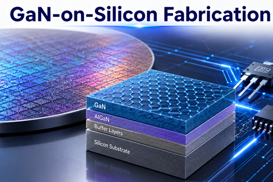
A typical GaN-on-silicon structure may contain:
- Silicon substrate – Provides mechanical support and a cost-effective manufacturing platform.
- Buffer layers – Reduce defects and manage stress between silicon and GaN.
- GaN epitaxial layer – Provides the primary semiconductor material for device formation.
- AlGaN layer – Used in many high-electron-mobility transistor (HEMT) structures to enable high-density electron channels.
- Metal contacts and dielectric layers – Form the electrical connections and insulation required for the finished device.
Carefully engineering these layers is essential for achieving high-quality GaN devices.
Why is GaN-on-Silicon Technology Important?
GaN offers properties that make it highly attractive for high-frequency and high-power applications. Combining GaN with silicon substrates can also provide significant manufacturing advantages.
Key benefits include:
- High electron mobility
- High breakdown field
- High-frequency operation
- Low switching losses
- High power density
- Improved energy efficiency
- Lower substrate cost compared with some alternative GaN substrates
- Compatibility with large-diameter wafer manufacturing
- Potential for high-volume semiconductor production
- Integration with established silicon manufacturing infrastructure
GaN-on-silicon is particularly valuable where high switching speed and power efficiency are more important than the traditional limitations of silicon-based power devices.
Technology Behind GaN-on-Silicon Fabrication
Manufacturing GaN-on-silicon devices requires precise epitaxial growth and process integration to control defects, stress, and electrical characteristics.
Epitaxial Growth
GaN layers are commonly deposited using techniques such as Metal-Organic Chemical Vapor Deposition (MOCVD). Precise control of temperature, pressure, gas flow, and precursor chemistry is required to produce uniform crystalline layers.
Buffer Engineering
Specially designed buffer structures are introduced between the silicon substrate and GaN layer. These layers help manage lattice mismatch, thermal stress, and unwanted electrical leakage.
Stress and Wafer Bow Control
Because GaN and silicon respond differently to temperature changes, thermal stress can cause wafer bow or cracking. Advanced multilayer structures and process optimization are used to maintain wafer integrity.
Device Fabrication
After epitaxial growth, conventional semiconductor processes such as lithography, deposition, etching, ion implantation, and metallization are used to form GaN transistors and other devices.
Advanced Metrology
X-ray diffraction, wafer-bow measurements, optical inspection, electrical characterization, and other metrology techniques are used to monitor crystal quality, layer thickness, defects, and device performance.
Together, these technologies enable reliable GaN device manufacturing on silicon substrates.
Applications
GaN-on-Silicon technology is increasingly important in applications where high efficiency, high switching frequency, and compact device size are required.
Major applications include:
- Fast-charging power adapters
- USB-C power supplies
- Data-center power systems
- Electric vehicle power electronics
- Renewable-energy systems
- RF and wireless communication
- 5G infrastructure
- Radar systems
- Aerospace and defense electronics
- High-efficiency DC-DC converters
- Consumer power electronics
Conclusion
GaN-on-Silicon Fabrication represents an important step toward making wide-bandgap semiconductor technology more scalable and cost-effective. By combining the superior electrical properties of GaN with the mature manufacturing ecosystem of silicon, the technology offers a powerful platform for high-frequency and high-efficiency electronic devices.
The major challenge remains controlling defects, wafer stress, thermal mismatch, and electrical leakage during GaN epitaxial growth. Continued advances in buffer engineering, epitaxy, wafer processing, and device fabrication are helping overcome these challenges.
As the semiconductor industry moves toward more efficient power conversion, faster RF systems, and compact high-performance electronics, GaN-on-Silicon will remain an important technology for the next generation of semiconductor devices.