

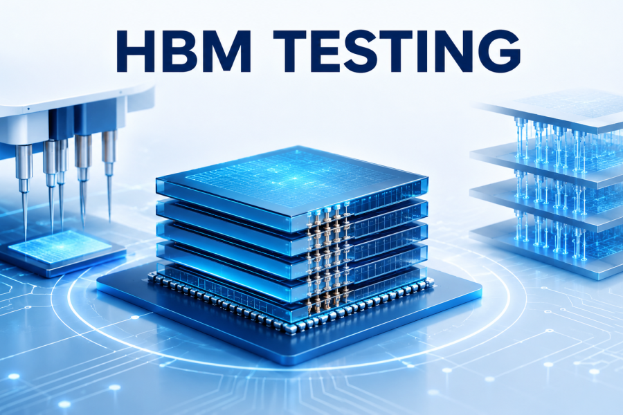
High-Bandwidth Memory (HBM) has become a critical technology for high-performance computing, artificial intelligence, graphics, and data-center accelerators. By stacking multiple DRAM dies vertically and connecting them through thousands of interconnects, HBM delivers significantly higher memory bandwidth within a compact package.
However, this highly integrated architecture also introduces complex testing challenges. HBM testing must verify individual memory dies, stacked components, interfaces, and the final package to ensure performance and reliability.
What Is HBM Testing?
HBM testing is the process of evaluating the electrical, functional, performance, and reliability characteristics of HBM devices throughout the semiconductor manufacturing and packaging flow.
Unlike conventional DRAM, HBM contains multiple vertically stacked memory dies connected through Through-Silicon Vias (TSVs) and microbumps. The large number of connections and high operating bandwidth require specialized test methodologies.
Testing can occur at several stages:
- Wafer-level testing
- Individual die testing
- Stack-level testing
- Package-level testing
- System-level validation
The objective is to detect defects as early as possible while ensuring that the completed HBM device meets its specifications.
Why Is HBM Testing Challenging?
HBM testing is considerably more complex than testing a conventional memory device because of its 3D architecture and extremely wide interface.
An HBM stack can contain multiple DRAM dies, with thousands of interconnects between the memory stack and the processor or accelerator.
Major challenges include:
High I/O Count
HBM uses a very wide interface to achieve high bandwidth. Testing these numerous signals requires sophisticated equipment and test strategies.
3D Stack Complexity
A defect inside one memory die, TSV, microbump, or interconnect can affect the functionality of the entire stack.
High-Speed Operation
Testing must verify that data can be transferred reliably at the required operating speeds.
Thermal Effects
High bandwidth and dense packaging can generate significant heat. Temperature-related behavior must therefore be evaluated during validation.
What Does HBM Testing Check?
A comprehensive HBM test program evaluates multiple aspects of the device.
Memory Functionality
Tests verify fundamental memory operations such as:
- Read and write operations
- Data retention
- Address decoding
- Memory-cell functionality
- Pattern-dependent failures
Electrical Parameters
Electrical testing can evaluate parameters such as:
- Voltage levels
- Leakage current
- Signal integrity
- Timing margins
- Power consumption
Interface Testing
The HBM interface must reliably communicate with the host processor or accelerator. Testing therefore examines signal behavior, timing, connectivity, and communication integrity.
Structural Testing
Specialized techniques can help identify defects in:
- TSVs
- Microbumps
- Interconnects
- Memory arrays
- Internal connections
The Future of HBM Testing
As HBM technology evolves toward higher bandwidth, greater capacity, and more advanced stacking, testing will become an increasingly important part of the overall packaging strategy.
Future challenges will involve balancing:
Higher Bandwidth + More Dies + More Interconnects + Thermal Constraints + Test Cost
Advanced analytics, improved DFT architectures, faster automated test equipment, and more sophisticated package-level validation will help address these challenges.
Conclusion
HBM testing is much more than checking whether a memory device can store and retrieve data. It requires verification of memory cells, high-speed interfaces, TSVs, microbumps, stacked dies, electrical behavior, thermal performance, and package-level functionality.
As AI accelerators and high-performance computing systems increasingly depend on HBM, robust testing will be essential for achieving the bandwidth, reliability, yield, and quality required by next-generation semiconductor systems.