

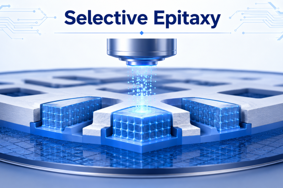
As semiconductor devices continue to shrink and architectures become increasingly complex, manufacturers need processes that can precisely control where and how semiconductor materials are grown. One technology playing an important role in this evolution is Selective Epitaxy.
Selective epitaxy enables crystalline semiconductor materials to grow only on specific regions of a wafer while minimizing or preventing growth on surrounding areas. This localized material growth provides greater control over device structures and supports the development of advanced transistor architectures.
What Is Selective Epitaxy?
Selective epitaxy is a semiconductor fabrication technique in which a crystalline semiconductor layer is grown selectively on exposed semiconductor surfaces while growth is suppressed on other materials, such as dielectric layers.
Unlike conventional blanket epitaxy, where material is deposited across a larger surface, selective epitaxy focuses growth precisely where it is required.
The process generally involves:
- Preparing the wafer surface
- Creating exposed semiconductor regions
- Using selective deposition chemistry
- Promoting epitaxial growth on the desired regions
- Suppressing unwanted deposition elsewhere
This approach allows engineers to build semiconductor structures with greater dimensional and material control.
Why Is Selective Epitaxy Important?
Modern semiconductor devices increasingly require three-dimensional structures and localized material engineering.
Selective epitaxy helps address these requirements by enabling engineers to add semiconductor material exactly where it is needed.
One major advantage is the ability to modify the geometry and electrical properties of transistor regions without applying the same material across the entire wafer.
This can support:
- Improved transistor performance
- Reduced parasitic effects
- Better strain engineering
- Precise source/drain formation
- More flexible device integration
- Continued technology scaling
In advanced logic technologies, these capabilities become increasingly valuable as conventional planar structures give way to more complex architectures.
Applications in Advanced Transistors
Selective epitaxy has become particularly important in the development of advanced transistor structures such as FinFETs and Gate-All-Around (GAA) devices.
For example, selective epitaxial growth can be used to form or enhance source/drain regions. Materials such as silicon-germanium or doped silicon can be selectively grown in specific transistor regions.
This enables strain engineering, where the lattice properties of the epitaxial material can influence carrier mobility and transistor performance.
In GAA and nanosheet-based architectures, selective epitaxy also contributes to the precise formation and engineering of three-dimensional device structures.
The Future of Selective Epitaxy
As semiconductor manufacturing moves toward smaller dimensions and increasingly three-dimensional architectures, selective epitaxy is expected to remain an important process technology.
Future developments will focus on improving:
- Atomic-level growth control
- Material selectivity
- Low-temperature processing
- Defect reduction
- Wafer-level uniformity
- Integration with advanced transistor architectures
Selective epitaxy is more than simply depositing semiconductor material. It is about controlling material growth with precision to build increasingly complex devices.
Conclusion
Selective epitaxy provides semiconductor manufacturers with precise control over localized crystal growth. By enabling targeted material formation, strain engineering, and advanced source/drain structures, it plays an important role in modern transistor fabrication.
As devices continue to evolve toward architectures such as GAA nanosheets and future 3D transistor designs, the ability to selectively engineer semiconductor materials will become even more critical.