

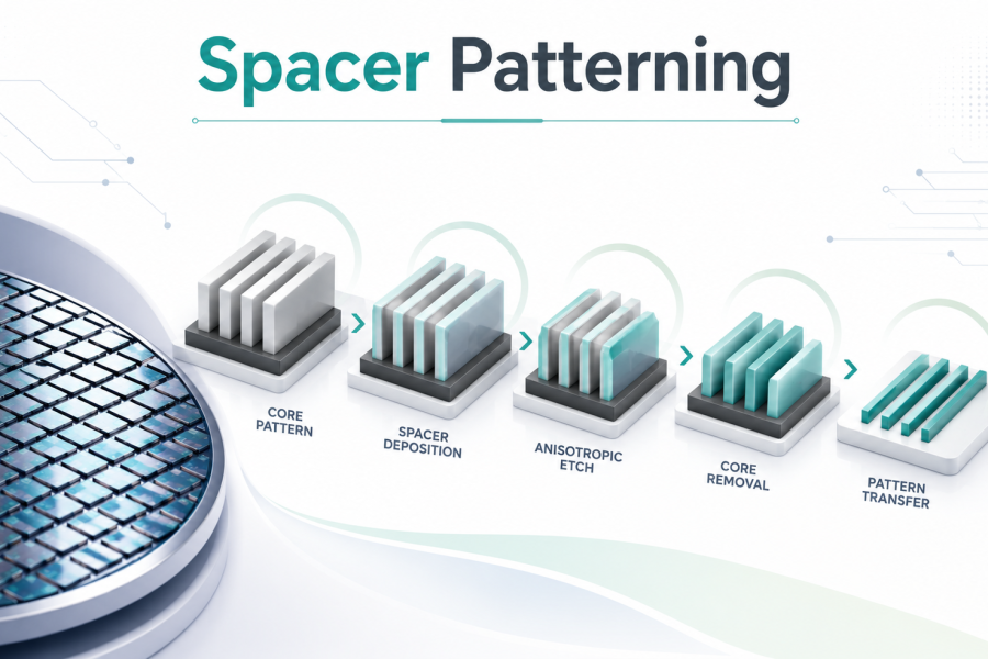
As semiconductor technology continues to scale toward smaller process nodes, conventional lithography techniques face increasing challenges in defining extremely small and closely spaced features. Spacer Patterning is an advanced patterning technique developed to overcome some of these limitations.
Instead of relying entirely on the resolution of the original lithography pattern, spacer-based techniques use precisely formed sidewall spacers to create additional features. This approach can effectively multiply the pattern density and support the fabrication of advanced semiconductor devices.
Spacer Patterning has therefore become an important concept in advanced lithography and nanoscale semiconductor manufacturing.
What Is Spacer Patterning?
Spacer Patterning is a semiconductor fabrication technique in which a thin material layer is deposited over a patterned structure and then etched anisotropically to leave material primarily along the structure’s sidewalls.
These remaining sidewall structures are called spacers.
The key advantage is that the final feature spacing can be determined by the thickness of the deposited spacer material rather than being limited entirely by the resolution of the lithography process used to create the original pattern.
Why Is Spacer Patterning Important?
Spacer Patterning provides several advantages for advanced semiconductor manufacturing:
- Higher pattern density: Enables smaller pitch structures.
- Improved uniformity: Self-aligned processes can provide consistent feature placement.
- Reduced overlay dependence: Multiple features can be generated from a common reference pattern.
- Enhanced scaling capability: Supports continued dimensional scaling in critical layers.
- Process flexibility: Spacer techniques can be integrated with different lithography and pattern-transfer approaches.
However, spacer-based processes also introduce challenges, including additional deposition and etching steps, tight film-thickness control, defect management, process complexity, and increasing manufacturing cost.
Applications
Spacer Patterning has played an important role in advanced semiconductor patterning, particularly for creating dense structures where pitch and critical-dimension control are extremely demanding.
Its concepts are relevant to applications such as advanced logic devices, memory technologies, FinFET-related structures, and other nanoscale semiconductor features.
As semiconductor dimensions continue to shrink, spacer-based techniques will remain an important part of the broader patterning toolbox. They can also work alongside advanced lithography technologies, including EUV, where appropriate, to achieve demanding patterning requirements.
Conclusion
Spacer Patterning demonstrates how semiconductor manufacturing can achieve increasingly dense structures by moving beyond conventional direct-printing approaches. By using precisely controlled sidewall spacers and self-aligned pattern formation, manufacturers can improve pattern density, dimensional control, and scalability.
As the semiconductor industry advances toward increasingly sophisticated process nodes, understanding spacer formation, self-aligned patterning, deposition, etching, and pattern transfer will be essential for anyone studying modern semiconductor fabrication.