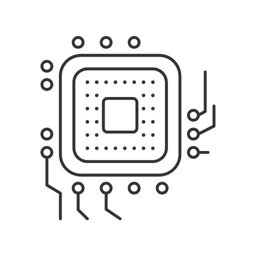


Printed Circuit Board design is a critical stage in electronic product development that directly impacts performance, reliability, and manufacturability. As electronic systems become faster, denser, and more complex, professional PCB design is essential to ensure signal integrity, power stability, and long-term product reliability. Avecas provides end-to-end PCB Design services that support a wide range of industries with high-quality, production-ready board designs.
Our PCB design solutions combine engineering precision, industry best practices, and manufacturing awareness to deliver boards that perform reliably from prototype to volume production.
We define PCB architecture based on system requirements, component placement strategies, and electrical constraints. Our engineers plan layer stackups, impedance targets, and routing strategies to ensure optimal signal and power performance. This structured planning stage minimizes design iterations and improves overall board quality.
Proper architecture ensures scalable and robust PCB designs.
Avecas provides accurate schematic capture services aligned with system functionality and component specifications. We perform thorough schematic reviews to identify potential design issues early, ensuring correct connectivity, power sequencing, and interface implementation.
Early validation helps reduce errors and accelerates development cycles.
Our PCB designers specialize in multilayer PCB layout for complex digital, analog, and mixed-signal systems. We apply best practices for high-speed routing, differential pairs, controlled impedance, and EMI reduction. Designs are optimized for performance, reliability, and manufacturability.
We support boards ranging from simple control systems to high-density, high-speed platforms.
Signal integrity and power integrity are critical for modern PCB designs. Avecas analyzes and optimizes signal paths, power distribution networks, and decoupling strategies to ensure stable operation. Our approach minimizes noise, crosstalk, and power fluctuations.
This results in improved system stability and performance.
We design PCBs with manufacturing and assembly in mind. Our engineers follow design for manufacturing and design for assembly guidelines to ensure smooth production. We generate complete fabrication and assembly documentation to support efficient manufacturing and reduce production risks.
This ensures a seamless transition from design to production.
Feel free to email us on below email address, we will be happy to answer your queries.
Your Partner for Reliable and Manufacturable PCB Solutions
Expertise across digital, analog, and mixed-signal designs.
Layouts optimized for fabrication, assembly, and testing.
Strong emphasis on signal integrity and power integrity.
PCB designs suitable for prototypes through high-volume production.
We support PCB design activities using industry-standard tools and proven methodologies to ensure high-quality, reliable, and manufacturable circuit board designs.
Advanced schematic capture and PCB layout tools used to develop accurate and scalable board designs.
Analysis techniques focused on maintaining signal quality and stable power delivery across high-speed designs.
Proven guidelines that ensure PCB designs are optimized for fabrication, assembly, and testing.
Structured validation and review processes that identify design issues early and improve production readiness.
designing advanced SoCs.
with specialized process needs.
demanding low-power solutions.
requiring safety-critical libraries.


PCB design involves creating schematics and layouts that define how electronic components are connected and mounted on a printed circuit board.
Yes. We design multilayer PCBs for complex digital, analog, and mixed-signal applications.
Do you provide manufacturing-ready PCB files?
Absolutely. Signal and power integrity optimization is a core part of our PCB design services.
Does Avecas offer end-to-end hardware support?