

Semiconductor R&D in India: The Role of IITs and IISc
IITs and IISc anchor India’s semiconductor research, driving indigenous chip design, fabrication access and the talent pipeline the industry depends on.
Tata Electronics’ Dholera Fab: India’s First 28nm-Class Foundry

A look at the Tata Electronics fab planned for Dholera, Gujarat, positioned as India’s first large-scale foundry aimed at mature 28nm-class process nodes.
India Semiconductor Mission Enters a New Phase with Strong Focus on Chip Design
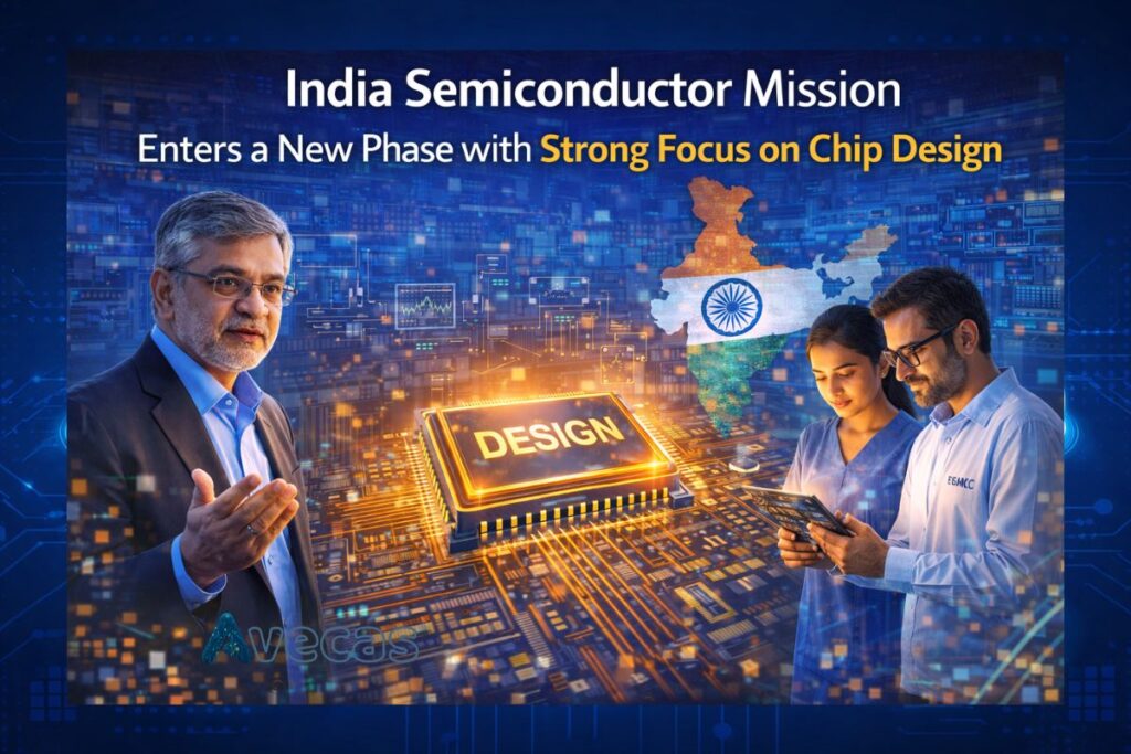
India’s semiconductor journey is entering a decisive new chapter as the government prepares to realign its strategy toward advanced chip design and innovation. Union Minister for Electronics and Information Technology Ashwini Vaishnaw recently highlighted that the next phase of the India Semiconductor Mission will place design capabilities at the center of the country’s technology roadmap. […]
Static Timing Analysis (STA) Explained Simply

Static timing analysis checks whether every signal in a chip arrives on time, without running simulations. Here is a clear, beginner-friendly explanation of how STA works.
HBM4 and the AI Memory Bottleneck

AI accelerators are increasingly limited not by compute but by memory bandwidth. HBM4 aims to widen that pipe, and the stakes for training clusters are considerable.
GlobalFoundries and the Case for Mature-Node Manufacturing

GlobalFoundries built its business around mature and specialty nodes rather than the leading edge, a strategy that highlights the enduring commercial value of established process technology.
India’s Role in the Global Chip Packaging Boom

India is positioning itself in the global chip packaging boom, where advanced assembly and test increasingly determine performance as transistor scaling slows.
Inside Sanand: India’s First OSAT/ATMP Facilities Take Shape in Gujarat

How Sanand in Gujarat became the launch point for India’s first assembly, test and packaging plants, and why back-end manufacturing came before leading-edge fabs.
What Is Physical Design? A Beginner’s Guide to the RTL-to-GDSII Flow

A beginner-friendly introduction to physical design, the stage of chip-making that turns register-transfer-level code into a manufacturable GDSII layout ready for the foundry.
Micron’s Gujarat Semiconductor Facility Set to Begin Commercial Chip Production, Strengthening India’s Make in India Vision

India’s ambitions to become a global semiconductor manufacturing hub are moving closer to reality as Micron Technology’s semiconductor facility in Sanand, Gujarat prepares to begin commercial chip production. The development marks a critical milestone in the country’s rapidly evolving semiconductor ecosystem and highlights the growing success of India’s “Make in India” and digital manufacturing initiatives. […]