

Fan-Out Wafer-Level Packaging (FOWLP): Powering Next-Generation Chips
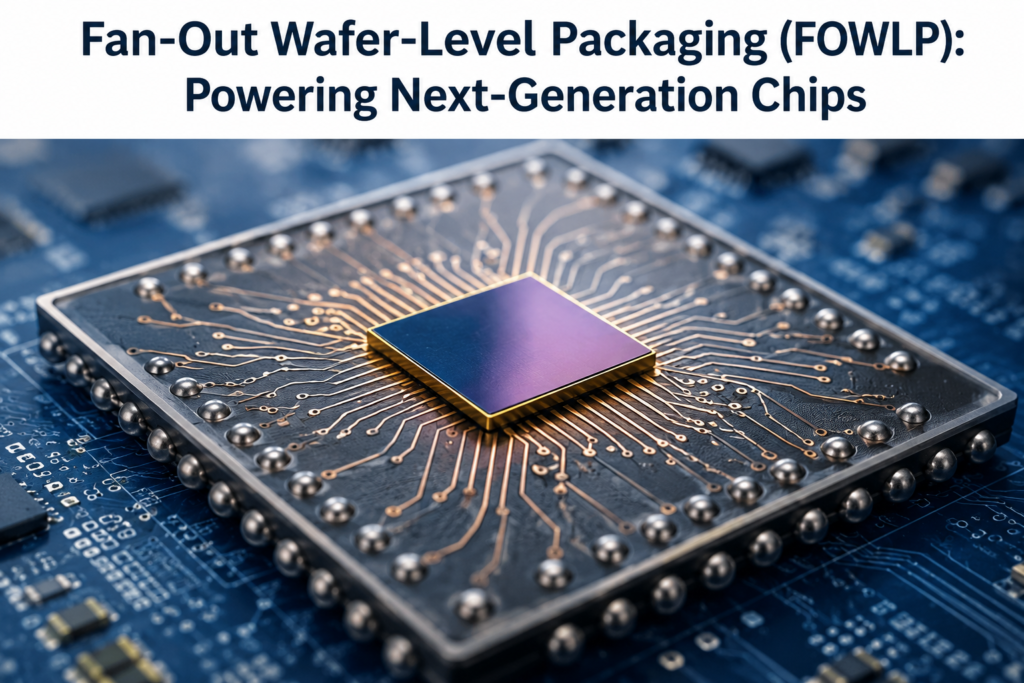
As semiconductor devices continue to evolve, the demand for higher performance, lower power consumption, and smaller form factors is growing rapidly. While transistor scaling remains important, advanced packaging technologies have become equally critical in driving innovation. One such technology is Fan-Out Wafer-Level Packaging (FOWLP), which is enabling the next generation of high-performance and compact electronic […]
2.5D vs 3D IC Packaging: Key Differences and Applications
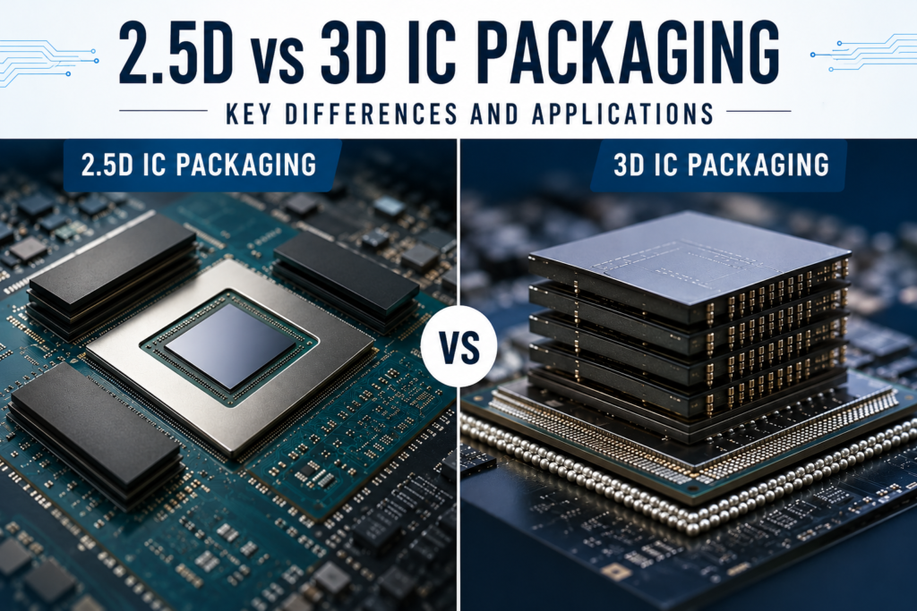
The semiconductor industry is continuously pushing the boundaries of performance, power efficiency, and integration. As traditional transistor scaling becomes increasingly challenging, advanced packaging technologies have emerged as a critical enabler of next-generation computing systems. Among these technologies, 2.5D IC Packaging and 3D IC Packaging have gained significant attention. Both approaches enable multiple semiconductor dies to […]
Beyond DRAM: The Emerging Memory Technologies Reshaping Computing

For decades, Dynamic Random Access Memory (DRAM) has been the workhorse of modern computing. From smartphones and laptops to AI accelerators and hyperscale data centers, DRAM provides the speed required for today’s demanding applications. However, the explosion of artificial intelligence, edge computing, autonomous systems, and cloud infrastructure is exposing DRAM’s limitations. High power consumption, volatility, […]
Advanced Floorplanning Strategies in Sub-7nm Designs

As we scale down to 5nm and 3nm nodes, floorplanning becomes a critical bottleneck. This post explores macro placement optimization, power grid design, and addressing IR-drop constraints at advanced nodes.
Mastering Static Timing Analysis (STA) Sign-Off for High-Frequency SoCs

Static Timing Analysis (STA) at 3GHz+ requires aggressive derating and multi-mode multi-corner (MMMC) optimization. We dive into OCV (On-Chip Variation), clock tree synthesis (CTS) balancing, and fixing setup/hold violations.
The Evolution of DFT: Scan Compression and LBIST in Complex ASICs

Design for Testability (DFT) is no longer an afterthought. With trillion-transistor chips, scan compression and Logic BIST (LBIST) are essential to reduce test time and maintain 99.9% fault coverage. Here is how modern DFT architectures are implemented.
UVM Verification: Best Practices for Scoreboards and Sequences

Universal Verification Methodology (UVM) remains the gold standard for ASIC verification. This guide breaks down advanced transaction-level modeling (TLM), sequence generation, and crafting robust scoreboards for zero-bug tape-outs.
Addressing Thermal and Power Dissipation in FinFET/GAAFET Architectures

Thermal throttling is a major issue in dense FinFET and GAAFET nodes. We discuss UPF (Unified Power Format) strategies, multi-Vt optimization, power gating, and dynamic voltage and frequency scaling (DVFS) for low-power SoCs.
Resolving Priority Inversion in RTOS-Based Embedded Architectures

Priority inversion is a silent, catastrophic bug in real-time operating systems. It occurs when a low-priority task holds a shared resource needed by a high-priority task, while a medium-priority task preempts the low-priority task, stalling the system. Indefinite Task Stalls and Hard-to-Reproduce Failures Priority inversion does not trigger immediate crashes. Instead, it causes intermittent timing […]
Resolving Priority Inversion in RTOS-Based Embedded Architectures

Priority inversion is a silent, catastrophic bug in real-time operating systems. It occurs when a low-priority task holds a shared resource needed by a high-priority task, while a medium-priority task preempts the low-priority task, stalling the system. Indefinite Task Stalls and Hard-to-Reproduce Failures Priority inversion does not trigger immediate crashes. Instead, it causes intermittent timing […]